4. ACPI Hardware Specification
ACPI defines standard interface mechanisms that allow an ACPI-compatible OS to control and communicate with an ACPI-compatible hardware platform. These interface mechanisms are optional (See “Hardware-Reduced ACPI”, below).However, if the ACPI Hardware Specification is implemented, platforms must comply with the requirements in this section.
This section describes the hardware aspects of ACPI.
ACPI defines “hardware” as a programming model and its behavior. ACPI strives to keep much of the existing legacy programming model the same; however, to meet certain feature goals, designated features conform to a specific addressing and programming scheme. Hardware that falls within this category is referred to as “fixed.”
Although ACPI strives to minimize these changes, hardware engineers should read this section carefully to understand the changes needed to convert a legacy-only hardware model to an ACPI/Legacy hardware model or an ACPI-only hardware model.
ACPI classifies hardware into two categories: Fixed or Generic. Hardware that falls within the fixed category meets the programming and behavior specifications of ACPI. Hardware that falls within the generic category has a wide degree of flexibility in its implementation.
4.1. Hardware-Reduced ACPI
For certain classes of systems the ACPI Hardware Specification may not be adequate. Examples include legacy-free, UEFI-based platforms with recent processors, and those implementing mobile platform architectures. For such platforms, a Hardware-reduced ACPI mode is defined. Under this definition, the ACPI Fixed Hardware interface is not implemented, and software alternatives for many of the features it supports are used instead. Note, though, that Hardware-reduced ACPI is not intended to support every possible ACPI system that can be built today. Rather, it is intended to introduce new systems that are designed to be HW-reduced from the start. The ACPI HW Specification should be used if the platform cannot be designed to work without it. Specifically, the following features are not supported under the HW-reduced definition:
The Global Lock, SMI_CMD, ACPI Enable and ACPI Disable. Hardware-reduced ACPI systems always boot in ACPI mode, and do not support hardware resource sharing between OSPM and other asynchronous operating environments, such as UEFI Runtime Services or System Management Mode.
Bus Master Reload and Arbiter Disable. Systems that depend on OS use of these bits to maintain cache coherency across processor sleep states are not supported.
GPE block devices are not supported.
Platforms that require the above features must implement the ACPI Hardware Specification.
Platforms that are designed for the Hardware-reduced ACPI definition must implement Revision 5 or greater of the Fixed ACPI Descriptor Table, and must set the HW_REDUCED_ACPI flag in the Flags field.
Note: FFH is permitted and applicable to both full and HW-reduced ACPI implementations.
4.1.1. Hardware-Reduced Events
HW-reduced ACPI platforms require alternatives to some of the features supported in the ACPI HW Specification, where none already exists. There are two areas that require such alternatives: The ACPI Platform Event Model, and System and Device Wakeup.
4.1.1.1. GPIO-Signaled Events or Interrupt Signaled Events
General Purpose Input/Output (GPIO) hardware can be used for signaling platform events. GPIO HW is a generalization of the GPE model, and is a shared hardware resource used for many applications. ACPI support for GPIO is described in section Connection Resources. ACPI 6.1 introduces the capability to signal events via interrupts. See Interrupt-signaled ACPI events for further details.
GPIO based event signaling is provided through GPIO interrupt connections, which describe the connection to a GPIO controller and pin, and which are mapped to the ACPI Event Handling mechanism via the ACPI Event Information namespace object (_AEI). OSPM treats GPIO Interrupt Connections listed in _AEI exactly as it does SCI interrupts: it executes the Event Method associated with the specific event. The name of the method to run is determined by the pin information contained in the GPIO Interrupt Connection resource. See GPIO-signaled ACPI Events for further details.
GPIO-signaled events can also be wake events, just as GPE events can on traditional ACPI platforms. Designating which events are wake events is done through attributes of the GPIO Interrupt Connection resource used.Devices may use _PRW to manage wake events as described in _PRW (Power Resources for Wake).
Interrupt based event signaling follows a similar methodology, a generic event device (GED) is declared which in turn describes all interrupts associated with event generation. The interrupts are listed in a _CRS object. When an interrupt is asserted the OSPM will execute the event method (_EVT) declared in the GED object specifying the interrupt identifier as a parameter. In this way the interrupt can be associated with specific platform events.
4.1.1.2. Interrupt-based Wake Events
Wake events on HW-reduced ACPI platforms are always caused by an interrupt reaching the processor. Therefore, there are two requirements for waking the system from a sleep or low-power idle state, or a device from a low-power state. First, the interrupt line must be Wake-Capable. Wake-capable interrupts are designed to be able to be delivered to the processor from low-power states. This implies that it must also cause the processor and any required platform hardware to power-up so that an Interrupt Service Routine can run. Secondly, an OS driver must enable the interrupt before entering a low-power state, or before OSPM puts the system into a sleep or low-power idle state.
Wake-capable interrupts are designated as such in their Extended Interrupt or GPIO Interrupt Connection resource descriptor.
4.2. Fixed Hardware Programming Model
Because of the changes needed for migrating legacy hardware to the fixed category, ACPI limits the features specified by fixed hardware. Fixed hardware features are defined by the following criteria:
Performance sensitive features
Features that drivers require during wake
Features that enable catastrophic OS software failure recovery
ACPI defines register-based interfaces to fixed hardware. CPU clock control and the power management timer are defined as fixed hardware to reduce the performance impact of accessing this hardware, which will result in more quickly reducing a thermal condition or extending battery life. If this logic were allowed to reside in PCI configuration space, for example, several layers of drivers would be called to access this address space. This takes a long time and will either adversely affect the power of the system (when trying to enter a low-power state) or the accuracy of the event (when trying to get a time stamp value).
Access to fixed hardware by OSPM allows OSPM to control the wake process without having to load the entire OS. For example, if PCI configuration space access is needed, the bus enumerator is loaded with all drivers used by the enumerator. Defining these interfaces in fixed hardware at addresses with which OSPM can communicate without any other driver’s assistance, allows OSPM to gather information prior to making a decision as to whether it continues loading the entire OS or puts it back to sleep.
If elements of the OS fail, it may be possible for OSPM to access address spaces that need no driver support. In such a situation, OSPM will attempt to honor fixed power button requests to transition the system to the G2 state. In the case where OSPM event handler is no longer able to respond to power button events, the power button override feature provides a back-up mechanism to unconditionally transition the system to the soft-off state.
4.3. Generic Hardware Programming Model
Although the fixed hardware programming model requires hardware registers to be defined at specific address locations, the generic hardware programming model allows hardware registers to reside in most address spaces and provides system OEMs with a wide degree of flexibility in the implementation of specific functions in hardware. OSPM directly accesses the fixed hardware registers, but relies on OEM-provided ACPI Machine Language (AML) code to access generic hardware registers.
AML code allows the OEM to provide the means for OSPM to control a generic hardware feature’s control and event logic.
The section entitled “ACPI Source Language Reference” describes the ACPI Source Language (ASL)–a programming language that OEMs use to create AML. The ASL language provides many of the operators found in common object-oriented programming languages, but it has been optimized to enable the description of platform power management and configuration hardware. An ASL compiler converts ASL source code to AML, which is a very compact machine language that the ACPI AML code interpreter executes.
AML does two things:
Abstracts the hardware from OSPM
Buffers OEM code from the different OS implementations
One goal of ACPI is to allow the OEM “value added” hardware to remain basically unchanged in an ACPI configuration. One attribute of value-added hardware is that it is all implemented differently. To enable OSPM to execute properly on different types of value added hardware, ACPI defines higher level “control methods” that it calls to perform an action. The OEM provides AML code, which is associated with control methods, to be executed by OSPM. By providing AML code, generic hardware can take on almost any form.
Another important goal of ACPI is to provide OS independence. To do this, the OEM AML code has to execute the same under any ACPI-compatible OS. ACPI allows for this by making the AML code interpreter part of OSPM. This allows OSPM to take care of synchronizing and blocking issues specific to each particular OS.
The generic feature model is represented in the following block diagram. In this model the generic feature is described to OSPM through AML code. This description takes the form of an object that sits in the ACPI Namespace associated with the hardware to which it is adding value.

Fig. 4.1 Generic Hardware Feature Model
As an example of a generic hardware control feature, a platform might be designed such that the IDE HDD’s D3 state has value-added hardware to remove power from the drive. The IDE drive would then have a reference to the AML PowerResource object (which controls the value added power plane) in its namespace, and associated with that object would be control methods that OSPM invokes to control the D3 state of the drive:
_PS0: A control method to sequence the IDE drive to the D0 state.
_PS3: A control method to sequence the IDE drive to the D3 state.
_PSC: A control method that returns the status of the IDE drive (on or off).
The control methods under this object provide an abstraction layer between OSPM and the hardware. OSPM understands how to control power planes (turn them on or off or to get their status) through its defined PowerResource object, while the hardware has platform-specific AML code (contained in the appropriate control methods) to perform the desired function. In this example, the platform would describe its hardware to the ACPI OS by writing and placing the AML code to turn the hardware off within the _PS3 control method. This enables the following sequence:
When OSPM decides to place the IDE drive in the D3 state, it calls the IDE driver and tells it to place the drive into the D3 state (at which point the driver saves the device’s context).
When the IDE driver returns control, OSPM places the drive in the D3 state.
OSPM finds the object associated with the HDD and then finds within that object any AML code associated with the D3 state.
OSPM executes the appropriate _PS3 control method to control the value-added “generic” hardware to place the HDD into an even lower power state.
As an example of a generic event feature, a platform might have a docking capability. In this case, it will want to generate an event. Notice that all ACPI events generate an SCI, which can be mapped to any shareable system interrupt. In the case of docking, the event is generated when a docking has been detected or when the user requests to undock the system. This enables the following sequence:
OSPM responds to the SCI and calls the AML code event handler associated with that generic event. The ACPI table associates the hardware event with the AML code event handler.
The AML-code event handler collects the appropriate information and then executes an AML Notify command to indicate to OSPM that a particular bus needs re-enumeration.
The following sections describe the fixed and generic hardware feature set of ACPI. These sections enable a reader to understand the following:
Which hardware registers are required or optional when an ACPI feature, concept or interface is required by a design guide for a platform class
How to design fixed hardware features
How to design generic hardware features
The ACPI Event Model
4.4. Diagram Legend
The hardware section uses simplified logic diagrams to represent how certain aspects of the hardware are implemented. The following symbols are used in the logic diagrams to represent programming bits:
 Write-only control bit
 Enable, control, or status bit
 Sticky status bit
 Query value
The half round symbol with an inverted “V” represents a write-only control bit. This bit has the behavior that it generates its control function when it is set. Reads to write-only bits are treated as ignore by software (the bit position is masked off and ignored).
The round symbol with an “X” represents a programming bit. As an enable or control bit, software setting or clearing this bit will result in the bit being read as set or clear (unless otherwise noted). As a status bit it directly represents the value of the signal.
The square symbol represents a sticky status bit. A sticky status bit is set by the level (not edge) of a hardware signal (active high or active low). The bit is only cleared by software writing a “1” to its bit position.
The rectangular symbol represents a query value from the embedded controller. This is the value the embedded controller returns to the system software upon a query command in response to an SCI event. The query value is associated with the event control method that is scheduled to execute upon an embedded controller event.
4.5. Register Bit Notation
Throughout this section there are logic diagrams that reference bits within registers. These diagrams use a notation that easily references the register name and bit position. The notation is as follows:
Registername.Bit
Registername contains the name of the register as it appears in this specification
Bit contains a zero-based decimal value of the bit position
For example, the SLP_EN bit resides in the PM1x_CNT register bit 13 and would be represented in diagram notation as:
SLP_ENPM1x_CNT.13
4.6. The ACPI Hardware Model
The ACPI hardware model is defined to allow OSPM to sequence the platform between the various global system states (G0-G3) as illustrated in the following figure by manipulating the defined interfaces. When first powered on, the platform finds itself in the global system state G3 or “Mechanical Off.” This state is defined as one where power consumption is very close to zero–the power plug has been removed; however, the real-time clock device still runs off a battery. The G3 state is entered by any power failure, defined as accidental or user-initiated power loss.
The G3 state transitions into either the G0 working state or the Legacy state depending on what the platform supports. If the platform is an ACPI-only platform, then it allows a direct boot into the G0 working state by always returning the status bit SCI_EN set (1) (for more information, see Legacy/ACPI Select and the SCI Interrupt). If the platform supports both legacy and ACPI operations (which is necessary for supporting a non-ACPI OS), then it would always boot into the Legacy state (illustrated by returning the SCI_EN clear (0)). In either case, a transition out of the G3 state requires a total boot of OSPM.
The Legacy system state is the global state where a non-ACPI OS executes. This state can be entered from either the G3 “Mechanical Off,” the G2 “Soft Off,” or the G0 “Working” states only if the hardware supports both Legacy and ACPI modes. In the Legacy state, the ACPI event model is disabled (no SCIs are generated) and the hardware uses legacy power management and configuration mechanisms. While in the Legacy state, an ACPI-compliant OS can request a transition into the G0 working state by performing an ACPI mode request. OSPM performs this transition by writing the ACPI_ENABLE value to the SMI_CMD, which generates an event to the hardware to transition the platform into ACPI mode. When hardware has finished the transition, it sets the SCI_EN bit and returns control back to OSPM. While in the G0 “working state,” OSPM can request a transition to Legacy mode by writing the ACPI_DISABLE value to the SMI_CMD register, which results in the hardware going into legacy mode and resetting the SCI_EN bit LOW (for more information, see Legacy/ACPI Select and the SCI Interrupt).
The G0 “Working” state is the normal operating environment of an ACPI system. In this state different devices are dynamically transitioning between their respective power states (D0, D1, D2, D3hot, or D3) and processors are dynamically transitioning between their respective power states (C0, C1, C2 or C3). In this state, OSPM can make a policy decision to place the platform into the system G1 “sleeping” state. The platform can only enter a single sleeping state at a time (referred to as the global G1 state); however, the hardware can provide up to four system sleeping states that have different power and exit latencies represented by the S1, S2, S3, or S4 states. When OSPM decides to enter a sleeping state it picks the most appropriate sleeping state supported by the hardware (OS policy examines what devices have enabled wake events and what sleeping states these support). OSPM initiates the sleeping transition by enabling the appropriate wake events and then programming the SLP_TYPx field with the desired sleeping state and then setting the SLP_ENx bit. The system will then enter a sleeping state; when one of the enabled wake events occurs, it will transition the system back to the working state (for more information, see Waking and Sleeping).
Another global state transition option while in the G0 “working” state is to enter the G2 “soft off” or the G3 “mechanical off” state. These transitions represent a controlled transition that allows OSPM to bring the system down in an orderly fashion (unloading applications, closing files, and so on). The policy for these types of transitions can be associated with the ACPI power button, which when pressed generates an event to the power button driver. When OSPM is finished preparing the operating environment for a power loss, it will either generate a pop-up message to indicate to the user to remove power, in order to enter the G3 “Mechanical Off” state, or it will initiate a G2 “soft-off” transition by writing the value of the S5 “soft off” system state to the SLP_TYPx register and setting the SLP_EN bit.
The G1 sleeping state is represented by four possible sleeping states that the hardware can support. Each sleeping state has different power and wake latency characteristics. The sleeping state differs from the working state in that the user’s operating environment is frozen in a low-power state until awakened by an enabled wake event. No work is performed in this state, that is, the processors are not executing instructions. Each system sleeping state has requirements about who is responsible for system context and wake sequences (for more information, see Waking and Sleeping).
The G2 “soft off” state is an OS initiated system shutdown. This state is initiated similar to the sleeping state transition (SLP_TYPx is set to the S5 value and setting the SLP_EN bit initiates the sequence). Exiting the G2 soft-off state requires rebooting the system. In this case, an ACPI-only system will re-enter the G0 state directly (hardware returns the SCI_EN bit set), while an ACPI/Legacy system transitions to the Legacy state (SCI_EN bit is clear).
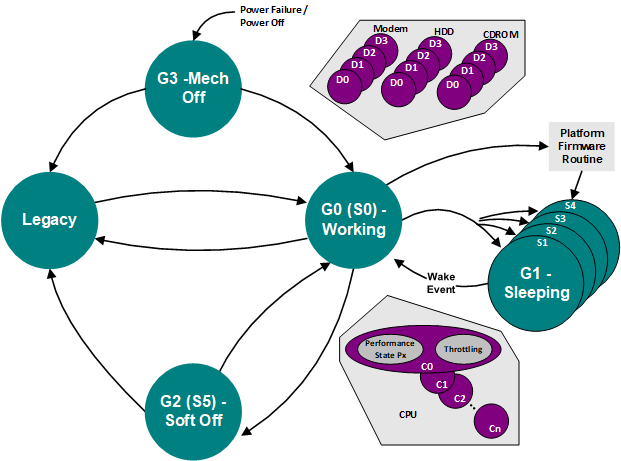
Fig. 4.2 Global States and Their Transitions
The ACPI architecture defines mechanisms for hardware to generate events and control logic to implement this behavior model. Events are used to notify OSPM that some action is needed, and control logic is used by OSPM to cause some state transition. ACPI-defined events are “hardware” or “interrupt” events. A hardware event is one that causes the hardware to unconditionally perform some operation. For example, any wake event will sequence the system from a sleeping state (S1, S2, S3, and S4 in the global G1 state) to the G0 working state (see Example Sleeping States).
An interrupt event causes the execution of an event handler (AML code or an ACPI-aware driver), which allows the software to make a policy decision based on the event. For ACPI fixed-feature events, OSPM or an ACPI-aware driver acts as the event handler. For generic logic events OSPM will schedule the execution of an OEM-supplied AML control method associated with the event.
For legacy systems, an event normally generates an OS-transparent interrupt, such as a System Management Interrupt, or SMI. For ACPI systems the interrupt events need to generate an OS-visible interrupt that is shareable; edge-style interrupts will not work. Hardware platforms that want to support both legacy operating systems and ACPI systems support a way of re-mapping the interrupt events between SMIs and SCIs when switching between ACPI and legacy models. This is illustrated in the following block diagram.

Fig. 4.3 Example Event Structure for a Legacy/ACPI Compatible Event Model
This example logic illustrates the event model for a sample platform that supports both legacy and ACPI event models. This example platform supports a number of external events that are power-related (power button, LID open/close, thermal, ring indicate) or Plug and Play-related (dock, status change). The logic represents the three different types of events:
OS Transparent Events
These events represent OEM-specific functions that have no OS support and use software that can be operated in an OS-transparent fashion (that is, SMIs).
Interrupt Events
These events represent features supported by ACPI-compatible operating systems, but are not supported by legacy operating systems. When a legacy OS is loaded, these events are mapped to the transparent interrupt (SMI# in this example), and when in ACPI mode they are mapped to an OS-visible shareable interrupt (SCI#). This logic is represented by routing the event logic through the decoder that routes the events to the SMI# arbiter when the SCI_EN bit is cleared, or to the SCI# arbiter when the SCI_EN bit is set.
Hardware events
These events are used to trigger the hardware to initiate some hardware sequence such as waking, resetting, or putting the system to sleep unconditionally.
In this example, the legacy power management event logic is used to determine device/system activity or idleness based on device idle timers, device traps, and the global standby timer. Legacy power management models use the idle timers to determine when a device should be placed in a low-power state because it is idle–that is, the device has not been accessed for the programmed amount of time. The device traps are used to indicate when a device in a low-power state is being accessed by OSPM. The global standby timer is used to determine when the system should be allowed to go into a sleeping state because it is idle–that is, the user interface has not been used for the programmed amount of time.
These legacy idle timers, trap monitors, and global standby timer are not used by OSPM in the ACPI mode. This work is handled by different software structures in an ACPI-compatible OS. For example, the driver model of an ACPI-compatible OS is responsible for placing its device into a low-power state (D1, D2, D3hot, or D3) and transitioning it back to the On state (D0) when needed. And OSPM is responsible for determining when the system is idle by profiling the system (using the PM Timer) and other knowledge it gains through its operating structure environment (which will vary from OS to OS). When the system is placed into the ACPI mode, these events no longer generate SMIs, as OSPM handles this function. These events are disabled through some OEM-proprietary method.
On the other hand, many of the hardware events are shared between the ACPI and legacy models (docking, the power button, and so on) and this type of interrupt event changes to an SCI event when enabled for ACPI. The ACPI OS will generate a request to the platform runtime firmware to enter into the ACPI mode. The firmware sets the SCI_EN bit to indicate that the system has successfully entered into the ACPI mode, so this is a convenient mechanism to map the desired interrupt (SMI or SCI) for these events (as shown in Figure 4-3).
The ACPI architecture specifies some dedicated hardware not found in the legacy hardware model: the power management timer (PM Timer). This is a free running timer that the ACPI OS uses to profile system activity. The frequency of this timer is explicitly defined in this specification and must be implemented as described.
Although the ACPI architecture reuses most legacy hardware as is, it does place restrictions on where and how the programming model is generated. If used, all fixed hardware features are implemented as described in this specification so that OSPM can directly access the fixed hardware feature registers.
Generic hardware features are manipulated by ACPI control methods residing in the ACPI Namespace. These interfaces can be very flexible; however, their use is limited by the defined ACPI control methods (for more information, see ACPI-Defined Devices and Device-Specific Objects). Generic hardware usually controls power planes, buffer isolation, and device reset resources. Additionally, “child” interrupt status bits can be accessed via generic hardware interfaces; however, they have a “parent” interrupt status bit in the GP_STS register. ACPI defines eight address spaces that may be accessed by generic hardware implementations. These include:
System I/O space
System memory space
PCI configuration space
Embedded controller space
System Management Bus (SMBus) space
CMOS
PCI BAR Target
IPMI space
Platform Communication Channel
Generic hardware power management features can be implemented accessing spare I/O ports residing in any of these address spaces. The ACPI specification defines an optional embedded controller and SMBus interfaces needed to communicate with these associated address spaces.
4.6.1. Hardware Reserved Bits
ACPI hardware registers are designed such that reserved bits always return zero, and data writes to them have no side affects. OSPM implementations must write zeros to reserved bits in enable and status registers and preserve bits in control registers, and they will treat these bits as ignored.
4.6.2. Hardware Ignored Bits
ACPI hardware registers are designed such that ignored bits are undefined and are ignored by software. Hardware-ignored bits can return zero or one. When software reads a register with ignored bits, it masks off ignored bits prior to operating on the result. When software writes to a register with ignored bit fields, it preserves the ignored bit fields.
4.6.3. Hardware Write-Only Bits
ACPI hardware defines a number of write-only control bits. These bits are activated by software writing a 1 to their bit position. Reads to write-only bit positions generate undefined results. Upon reads to registers with write-only bits, software masks out all write-only bits.
4.6.4. Cross Device Dependencies
Cross Device Dependency is a condition in which an operation to a device interferes with the operation of other unrelated devices, or allows other unrelated devices to interfere with its behavior. This condition is not supportable and can cause platform failures. ACPI provides no support for cross device dependencies and suggests that devices be designed to not exhibit this behavior. The following two examples describe cross device dependencies:
4.7. ACPI Hardware Features
This section describes the different hardware features defined by the ACPI interface. These features are categorized as the following:
Fixed Hardware Features
Generic Hardware Features
Fixed hardware features reside in a number of the ACPI-defined address spaces at the locations described by the ACPI programming model. Generic hardware features reside in one of four address spaces (system I/O, system memory, PCI configuration, embedded controller, or serial device I/O space) and are described by the ACPI Namespace through the declaration of AML control methods.
Fixed hardware features have exact definitions for their implementation. Although many fixed hardware features are optional, if implemented they must be implemented as described since OSPM manipulates the registers of fixed hardware devices and expects the defined behavior. Functional fixed hardware provides functional equivalents of the fixed hardware feature interfaces as described in Generic Hardware Programming Model
Generic hardware feature implementation is flexible. This logic is controlled by OEM-supplied AML code (for more information, see ACPI Software Programming Model ), which can be written to support a wide variety of hardware. Also, ACPI provides specialized control methods that provide capabilities for specialized devices. For example, the Notify command can be used to notify OSPM from a generic hardware event handler (control method) that a docking or thermal event has taken place. A good understanding of this section and ACPI Software Programming Model of this specification will give designers a good understanding of how to design hardware to take full advantage of an ACPI-compatible OS.
Notice that the generic features are listed for illustration only, the ACPI specification can support many types of hardware not listed.
Feature Name |
Description |
Programming Model |
|---|---|---|
Power Management Timer |
24-bit or 32-bit free running timer. |
Fixed Hardware Feature Control Logic |
Power Button |
User pushes button to switch the system between the working and sleeping/soft-off states. |
Fixed Hardware Event and Control Logic or Generic Hardware Event and Logic |
Sleep Button |
User pushes button to switch the system between the working and sleeping/soft-off states. |
Fixed Hardware Event and Control Logic or Generic Hardware Event and Logic |
Power Button Override |
User sequence (press the power button for at least 4 seconds) to turn off a hung system. |
|
Real Time Clock Alarm |
Programmed time to wake the system. |
Optional Fixed Hardware* |
Sleep/Wake Control Logic |
Logic used to transition the system between the sleeping and working states. |
Fixed Hardware Control and Event Logic |
Embedded Controller Interface |
ACPI Embedded Controller protocol and interface, as described in the ACPI Embedded Controller Interface Specification. |
Generic Hardware Event Logic, must reside in the general-purpose register block |
Legacy/ACPI Select |
Status bit that indicates the system is using the legacy or ACPI power management model (SCI_EN). |
Fixed Hardware Control Logic |
Lid switch |
Button used to indicate whether the system’s lid is open or closed (mobile systems only) |
Generic Hardware Event Feature |
C1 Power State |
Processor instruction to place the processor into a low-power state. |
Processor ISA |
C2 Power Control |
Logic to place the processor into a C2 power state. |
Fixed Hardware Control Logic |
C3 Power Control |
Logic to place the processor into a C3 power state. |
Fixed Hardware Control Logic |
Thermal Control |
Logic to generate thermal events at specified trip points. |
Generic Hardware Event and Control Logic (See description of thermal logic in Thermal Management Concepts) |
Device Power Management |
Control logic for switching between different device power states. |
Generic Hardware control logic |
AC Adapter |
Logic to detect the insertion and removal of the AC adapter. |
Generic Hardware event logic |
Docking/device insertion and removal |
Logic to detect device insertion and removal events. |
Generic Hardware event logic |
* RTC wakeup alarm is required; the fixed hardware feature status bit is optional.
4.8. ACPI Register Model
ACPI hardware resides in one of six address spaces:
System I/O
System memory
PCI configuration
SMBus
Embedded controller
Functional Fixed Hardware
Different implementations will result in different address spaces being used for different functions. The ACPI specification consists of fixed hardware registers and generic hardware registers. Fixed hardware registers are required to implement ACPI-defined interfaces. The generic hardware registers are needed for any events generated by value-added hardware.
ACPI defines register blocks. An ACPI-compatible system provides an ACPI table (the FADT, built in memory at boot-up) that contains a list of pointers to the different fixed hardware register blocks used by OSPM. The bits within these registers have attributes defined for the given register block. The types of registers that ACPI defines are:
Status/Enable Registers (for events)
Control Registers
If a register block is of the status/enable type, then it will contain a register with status bits, and a corresponding register with enable bits. The status and enable bits have an exact implementation definition that needs to be followed (unless otherwise noted), which is illustrated by the following diagram:

Fig. 4.4 Block Diagram of a Status/Enable Cell
Notice that the status bit, which hardware sets by the Event Input being set in this example, can only be cleared by software writing a 1 to its bit position. Also, the enable bit has no effect on the setting or resetting of the status bit; it only determines if the SET status bit will generate an “Event Output,” which generates an SCI when set if its enable bit is set.
ACPI also defines register groupings. A register grouping consists of two register blocks, with two pointers to two different blocks of registers, where each bit location within a register grouping is fixed and cannot be changed. The bits within a register grouping, which have fixed bit positions, can be split between the two register blocks. This allows the bits within a register grouping to reside in either or both register blocks, facilitating the ability to map bits within several different chips to the same register thus providing the programming model with a single register grouping bit structure.
OSPM treats a register grouping as a single register; but located in multiple places. To read a register grouping, OSPM will read the “A” register block, followed by the “B” register block, and then will logically “OR” the two results together (the SLP_TYP field is an exception to this rule). Reserved bits, or unused bits within a register block always return zero for reads and have no side effects for writes (which is a requirement).
The SLP_TYPx field can be different for each register grouping. The respective sleeping object \_Sx contains a SLP_TYPa and a SLP_TYPb field. That is, the object returns a package with two integer values of 0-7 in it. OSPM will always write the SLP_TYPa value to the “A” register block followed by the SLP_TYPb value within the field to the “B” register block. All other bit locations will be written with the same value. Also, OSPM does not read the SLP_TYPx value but throws it away.
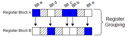
Fig. 4.5 Example Fixed Hardware Feature Register Grouping
As an example, the above diagram represents a register grouping consisting of register block A and register block b. Bits “a” and “d” are implemented in register block B and register block A returns a zero for these bit positions. Bits “b”, “c” and “e” are implemented in register block A and register block B returns a zero for these bit positions. All reserved or ignored bits return their defined ACPI values.
When accessing this register grouping, OSPM must read register block a, followed by reading register block b. OSPM then does a logical OR of the two registers and then operates on the results.
When writing to this register grouping, OSPM will write the desired value to register group A followed by writing the same value to register group B.
ACPI defines the following fixed hardware register blocks. Each register block gets a separate pointer from the FADT. These addresses are set by the OEM as static resources, so they are never changed–OSPM cannot re-map ACPI resources. The following register blocks are defined:
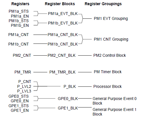
Fig. 4.6 Register Blocks versus Register Groupings
The PM1 EVT grouping consists of the PM1a_EVT and PM1b_EVT register blocks, which contain the fixed hardware feature event bits. Each event register block (if implemented) contains two registers: a status register and an enable register. Each register grouping has a defined bit position that cannot be changed; however, the bit can be implemented in either register block (A or B). The A and B register blocks for the events allow chipsets to vary the partitioning of events into two or more chips. For read operations, OSPM will generate a read to the associated A and B registers, OR the two values together, and then operate on this result. For write operations, OSPM will write the value to the associated register in both register blocks. Therefore, there are two rules to follow when implementing event registers:
Reserved or unimplemented bits always return zero (control or enable).
Writes to reserved or unimplemented bits have no affect.
The PM1 CNT grouping contains the fixed hardware feature control bits and consists of the PM1a_CNT_BLK and PM1b_CNT_BLK register blocks. Each register block is associated with a single control register. Each register grouping has a defined bit position that cannot be changed; however, the bit can be implemented in either register block (A or B). There are two rules to follow when implementing CNT registers:
Reserved or unimplemented bits always return zero (control or enable).
Writes to reserved or unimplemented bits have no affect.
The PM2_CNT_BLK register block currently contains a single bit for the arbiter disable function. The general-purpose event register contains the event programming model for generic features. All generic events, just as fixed events, generate SCIs. Generic event status bits can reside anywhere; however, the top-level generic event resides in one of the general-purpose register blocks. Any generic feature event status not in the general-purpose register space is considered a child or sibling status bit, whose parent status bit is in the general-purpose event register space. Notice that it is possible to have N levels of general-purpose events prior to hitting the GPE event status.
General-purpose event registers are described by two register blocks: The GPE0_BLK or the GPE1_BLK. Each register block is pointed to separately from within the FADT. Each register block is further broken into two registers: GPEx_STS and GPEx_EN. The status and enable registers in the general-purpose event registers follow the event model for the fixed hardware event registers.
4.8.1. ACPI Register Summary
The following tables summarize the ACPI registers:
Register |
Size (Bytes) |
Address (relative to register block) |
|---|---|---|
PM1a_STS |
PM1_EVT_LEN/2 |
<PM1a_EVT_BLK> |
PM1a_EN |
PM1_EVT_LEN/2 |
<PM1a_EVT_BLK>+PM1_EVT_LEN/2 |
PM1b_STS |
PM1_EVT_LEN/2 |
<PM1b_EVT_BLK> |
PM1b_EN |
PM1_EVT_LEN/2 |
<PM1b_EVT_BLK>+PM1_EVT_LEN/2 |
Register |
Size (Bytes) |
Address (relative to register block) |
|---|---|---|
PM1_CNTa |
PM1_CNT_LEN |
<PM1a_CNT_BLK> |
PM1_CNTb |
PM1_CNT_LEN |
<<PM1b_CNT_BLK> |
Register |
Size (Bytes) |
Address (relative to register block) |
|---|---|---|
PM2_CNT |
PM2_CNT_LEN |
<PM2_CNT_BLK> |
Register |
Size (Bytes) |
Address (relative to register block) |
|---|---|---|
PM_TMR |
PM_TMR_LEN |
<PM_TMR_BLK> |
Register |
Size (Bytes) |
Address (relative to register block) |
|---|---|---|
P_CNT |
4 |
Either <P_BLK> or specified by the PTC object - see Processor Throttling Controls |
P_LVL2 |
1 |
<P_BLK>+4h |
P_LVL3 |
1 |
<P_BLK>+5h |
Register |
Size (Bytes) |
Address (relative to register block) |
|---|---|---|
GPE0_STS |
GPE0_LEN/2 |
<GPE0_BLK> |
GPE0_EN |
GPE0_LEN/2 |
<GPE0_BLK>+GPE0_LEN/2 |
GPE1_STS |
GPE1_LEN/2 |
<GPE1_BLK> |
GPE1_EN |
GPE1_LEN/2 |
<GPE1_BLK>+GPE1_LEN/2 |
4.8.1.1. PM1 Event Registers
The PM1 event register grouping contains two register blocks: the PM1a_EVT_BLK is a required register block when the following ACPI interface categories are required by a class specific platform design guide:
Power management timer control/status
Processor power state control/status
Global Lock related interfaces
Power or Sleep button (fixed register interfaces)
System power state controls (sleeping/wake control)
The PM1b_EVT_BLK is an optional register block. Each register block has a unique 32-bit pointer in the Fixed ACPI Table (FADT) to allow the PM1 event bits to be partitioned between two chips. If the PM1b_EVT_BLK is not supported, its pointer contains a value of zero in the FADT.
Each register block in the PM1 event grouping contains two registers that are required to be the same size: the PM1x_STS and PM1x_EN (where x can be “a” or “b”). The length of the registers is variable and is described by the PM1_EVT_LEN field in the FADT, which indicates the total length of the register block in bytes. Hence if a length of “4” is given, this indicates that each register contains two bytes of I/O space. The PM1 event register block has a minimum size of 4 bytes.
4.8.1.2. PM1 Control Registers
The PM1 control register grouping contains two register blocks: the PM1a_CNT_BLK is a required register block when the following ACPI interface categories are required by a class specific platform design guide:
SCI/SMI routing control/status for power management and general-purpose events
Processor power state control/status
Global Lock related interfaces
System power state controls (sleeping/wake control)
The PM1b_CNT_BLK is an optional register block. Each register block has a unique 32-bit pointer in the Fixed ACPI Table (FADT) to allow the PM1 event bits to be partitioned between two chips. If the PM1b_CNT_BLK is not supported, its pointer contains a value of zero in the FADT.
Each register block in the PM1 control grouping contains a single register: the PM1x_CNT. The length of the register is variable and is described by the PM1_CNT_LEN field in the FADT, which indicates the total length of the register block in bytes. The PM1 control register block must have a minimum size of 2 bytes.
4.8.1.3. PM2 Control Register
The PM2 control register is contained in the PM2_CNT_BLK register block. The FADT contains a length variable for this register block (PM2_CNT_LEN) that is equal to the size in bytes of the PM2_CNT register (the only register in this register block). This register block is optional, if not supported its block pointer and length contain a value of zero.
4.8.1.4. PM Timer Register
The PM timer register is contained in the PM_TMR_BLK register block. It is an optional register block that must be implemented when the power management timer control/status ACPI interface category is required by a class specific platform design guide.
If defined, this register block contains the register that returns the running value of the power management timer. The FADT also contains a length variable for this register block (PM_TMR_LEN) that is equal to the size in bytes of the PM_TMR register (the only register in this register block).
4.8.1.5. Processor Control Block (P_BLK)
There is an optional processor control register block for each processor in the system. As this is a homogeneous feature, all processors must have the same level of support. The ACPI OS will revert to the lowest common denominator of processor control block support. The processor control block contains the processor control register (P_CNT-a 32-bit performance control configuration register), and the P_LVL2 and P_LVL3 CPU sleep state control registers. The 32-bit P_CNT register controls the behavior of the processor clock logic for that processor, the P_LVL2 register is used to place the CPU into the C2 state, and the P_LVL3 register is used to place the processor into the C3 state.
4.8.1.6. General-Purpose Event Registers
The general-purpose event registers contain the root level events for all generic features. To facilitate the flexibility of partitioning the root events, ACPI provides for two different general-purpose event blocks: GPE0_BLK and GPE1_BLK. These are separate register blocks and are not a register grouping, because there is no need to maintain an orthogonal bit arrangement. Also, each register block contains its own length variable in the FADT, where GPE0_LEN and GPE1_LEN represent the length in bytes of each register block.
Each register block contains two registers of equal length: GPEx_STS and GPEx_EN (where x is 0 or 1). The length of the GPE0_STS and GPE0_EN registers is equal to half the GPE0_LEN. The length of the GPE1_STS and GPE1_EN registers is equal to half the GPE1_LEN. If a generic register block is not supported then its respective block pointer and block length values in the FADT table contain zeros. The GPE0_LEN and GPE1_LEN do not need to be the same size.
4.8.2. Fixed Hardware Features
This section describes the fixed hardware features defined by ACPI.
4.8.2.1. Power Management Timer
The ACPI specification defines an optional power management timer that provides an accurate time value that can be used by system software to measure and profile system idleness (along with other tasks). The power management timer provides an accurate time function while the system is in the working (G0) state. To allow software to extend the number of bits in the timer, the power management timer generates an interrupt when the last bit of the timer changes (from 0 to 1 or 1 to 0). ACPI supports either a 24-bit or 32-bit power management timer. The PM Timer is accessed directly by OSPM, and its programming model is contained in fixed register space. The programming model can be partitioned in up to three different register blocks. The event bits are contained in the PM1_EVT register grouping, which has two register blocks, and the timer value can be accessed through the PM_TMR_BLK register block. A block diagram of the power management timer is illustrated in the following figure.
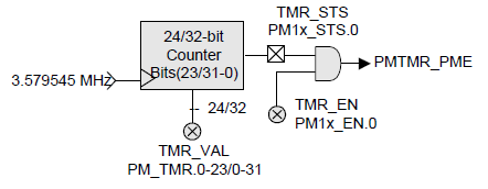
Fig. 4.7 Power Management Timer
The power management timer is a 24-bit or 32-bit fixed rate free running count-up timer that runs off a 3.579545 MHz clock. The ACPI OS checks the FADT to determine whether the PM Timer is a 32-bit or 24-bit timer. The programming model for the PM Timer consists of event logic, and a read port to the counter value. The event logic consists of an event status and enable bit. The status bit is set any time the last bit of the timer (bit 23 or bit 31) goes from set to clear or clear to set. If the TMR_EN bit is set, then the setting of the TMR_STS will generate an ACPI event in the PM1_EVT register grouping (referred to as PMTMR_PME in the diagram). The event logic is only used to emulate a larger timer.
OSPM uses the read-only TMR_VAL field (in the PM TMR register grouping) to read the current value of the timer. OSPM never assumes an initial value of the TMR_VAL field; instead, it reads an initial TMR_VAL upon loading OSPM and assumes that the timer is counting. It is allowable to stop the Timer when the system transitions out of the working (G0/S0) state. The only timer reset requirement is that the timer functions while in the working state.
The PM Timer’s programming model is implemented as a fixed hardware feature to increase the accuracy of reading the timer.
4.8.2.2. Console Buttons
ACPI defines user-initiated events to request OSPM to transition the platform between the G0 working state and the G1 sleeping, G2 soft off and G3 mechanical off states. ACPI also defines a recommended mechanism to unconditionally transition the platform from a hung G0 working state to the G2 soft-off state.
ACPI operating systems use power button events to determine when the user is present. As such, these ACPI events are associated with buttons in the ACPI specification.
The ACPI specification supports two button models:
A single-button model that generates an event for both sleeping and entering the soft-off state. The function of the button can be configured using OSPM UI.
A dual-button model where the power button generates a soft-off transition request and a sleep button generates a sleep transition request. The type of button implies the function of the button.
Control of these button events is either through the fixed hardware programming model or the generic hardware programming model (control method based). The fixed hardware programming model has the advantage that OSPM can access the button at any time, including when the system is crashed. In a crashed system with a fixed hardware power button, OSPM can make a “best” effort to determine whether the power button has been pressed to transition to the system to the soft-off state, because it doesn’t require the AML interpreter to access the event bits.
4.8.2.2.1. Power Button
The power button logic can be used in one of two models: single button or dual button. In the single-button model, the user button acts as both a power button for transitioning the system between the G0 and G2 states and a sleep button for transitioning the system between the G0 and G1 states. The action of the user pressing the button is determined by software policy or user settings. In the dual-button model, there are separate buttons for sleeping and power control. Although the buttons still generate events that cause software to take an action, the function of the button is now dedicated: the sleep button generates a sleep request to OSPM and the power button generates a wake request.
Support for a power button is indicated by a combination of the PWR_BUTTON flag and the power button device object, as shown in the following:
Indicated Support |
PWR_BUTTON Flag |
Power Button Device Object |
|---|---|---|
Fixed hardware power button |
Clear |
Absent |
Control method power button |
Set |
Present |
The power button can also have an additional capability to unconditionally transition the system from a hung working state to the G2 soft-off state. In the case where OSPM event handler is no longer able to respond to power button events, the power button override feature provides a back-up mechanism to unconditionally transition the system to the soft-off state. This feature can be used when the platform doesn’t have a mechanical off button, which can also provide this function. ACPI defines that holding the power button active for four seconds or longer will generate a power button override event.
4.8.2.2.1.1. Fixed Power Button
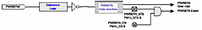
Fig. 4.8 Fixed Power Button Logic
The fixed hardware power button has its event programming model in the PM1x_EVT_BLK. This logic consists of a single enable bit and sticky status bit. When the user presses the power button, the power button status bit (PWRBTN_STS) is unconditionally set. If the power button enable bit (PWRBTN_EN) is set and the power button status bit is set (PWRBTN_STS) due to a button press while the system is in the G0 state, then an SCI is generated. OSPM responds to the event by clearing the PWRBTN_STS bit. The power button logic provides debounce logic that sets the PWRBTN_STS bit on the button press “edge.”
While the system is in the G1 or G2 global states (S1, S2, S3, S4 or S5 states), any further power button press after the button press that transitioned the system into the sleeping state unconditionally sets the power button status bit and wakes the system, regardless of the value of the power button enable bit. OSPM responds by clearing the power button status bit and waking the system.
4.8.2.2.1.2. Control Method Power Button
The power button programming model can also use the generic hardware programming model. This allows the power button to reside in any of the generic hardware address spaces (for example, the embedded controller) instead of fixed space. If the power button is implemented using generic hardware, then the OEM needs to define the power button as a device with an _HID object value of “PNP0C0C,” which then identifies this device as the power button to OSPM. The AML event handler then generates a Notify command to notify OSPM that a power button event was generated. While the system is in the working state, a power button press is a user request to transition the system into either the sleeping (G1) or soft-off state (G2). In these cases, the power button event handler issues the Notify command with the device specific code of 0x80. This indicates to OSPM to pass control to the power button driver (PNP0C0C) with the knowledge that a transition out of the G0 state is being requested. Upon waking from a G1 sleeping state, the AML event handler generates a notify command with the code of 0x2 to indicate it was responsible for waking the system.
The power button device needs to be declared as a device within the ACPI Namespace for the platform and only requires an _HID. An example definition follows.
This example ASL code performs the following:
Creates a device named “PWRB” and associates the Plug and Play identifier (through the _HID object) of “PNP0C0C.”
The Plug and Play identifier associates this device object with the power button driver.
Creates an operational region for the control method power button’s programming model: System I/O space at 0x200.
Fields that are not accessed are written as zeros. These status bits clear upon writing a 1 to their bit position, therefore preserved would fail in this case.
Creates a field within the operational region for the power button status bit (called PBP). In this case the power button status bit is a child of the general-purpose event status bit 0. When this bit is set, it is the responsibility of the ASL-code to clear it (OSPM clears the general-purpose status bits). The address of the status bit is 0x200.0 (bit 0 at address 0x200).
Creates an additional status bit called PBW for the power button wake event. This is the next bit and its physical address would be 0x200.1 (bit 1 at address 0x200).
Generates an event handler for the power button that is connected to bit 0 of the general-purpose event status register 0. The event handler does the following:
Clears the power button status bit in hardware (writes a one to it).
Notifies OSPM of the event by calling the Notify command passing the power button object and the device specific event indicator 0x80.
// Define a control method power button
Device(\_SB.PWRB)
{
    Name(_HID, EISAID("PNP0C0C"))
    Name(_PRW, Package(){0, 0x4})
    OperationRegion(\PHO, SystemIO, 0x200, 0x1)
    Field(\PHO, ByteAcc, NoLock, WriteAsZeros)
    {
        PBP, 1,                      // sleep/off request
        PBW, 1                       // wakeup request
    }
}

Scope(\_GPE)                         // Root level event handlers
{
    Method(_L00)
    {
        // uses bit 0 of GP0_STS register
        If (PBP)
        {
            PBP = One                // clear power button status
            Notify(\_SB.PWRB, 0x80)  // Notify OS of event
        }

        If (\PBW)
        {
           PBW = One
           Notify(\_SB.PWRB, 0x2)
        }
    }
}
4.8.2.2.1.3. Power Button Override
The ACPI specification also allows that if the user presses the power button for more than four seconds while the system is in the working state, a hardware event is generated and the system will transition to the soft-off state. This hardware event is called a power button override. In reaction to the power button override event, the hardware clears the power button status bit (PWRBTN_STS).
4.8.2.2.2. Sleep Button
When using the two button model, ACPI supports a second button that when pressed will request OSPM to transition the platform between the G0 working and G1 sleeping states. Support for a sleep button is indicated by a combination of the SLEEP_BUTTON flag and the sleep button device object:
Indicated Support |
SLEEP_BUTTON Flag |
Sleep Button Device Object |
|---|---|---|
No sleep button |
Set |
Absent |
Fixed hardware slee button |
Clear |
Absent |
Control method sleep button |
Set |
Present |
4.8.2.2.2.1. Fixed Hardware Sleep Button
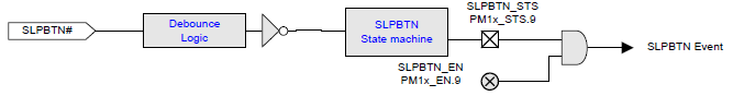
Fig. 4.9 Fixed Hardware Sleep Button Logic
The fixed hardware sleep button has its event programming model in the PM1x_EVT_BLK. This logic consists of a single enable bit and sticky status bit. When the user presses the sleep button, the sleep button status bit (SLPBTN_STS) is unconditionally set. Additionally, if the sleep button enable bit (SLPBTN_EN) is set, and the sleep button status bit is set (SLPBTN_STS, due to a button press) while the system is in the G0 state, then an SCI is generated. OSPM responds to the event by clearing the SLPBTN_STS bit. The sleep button logic provides debounce logic that sets the SLPBTN_STS bit on the button press “edge.”
While the system is sleeping (in either the S0, S1, S2, S3 or S4 states), any further sleep button press (after the button press that caused the system transition into the sleeping state) sets the sleep button status bit (SLPBTN_STS) and wakes the system if the SLP_EN bit is set. OSPM responds by clearing the sleep button status bit and waking the system.
4.8.2.2.2.2. Control Method Sleep Button
The sleep button programming model can also use the generic hardware programming model. This allows the sleep button to reside in any of the generic hardware address spaces (for example, the embedded controller) instead of fixed space. If the sleep button is implemented via generic hardware, then the OEM needs to define the sleep button as a device with an _HID object value of “PNP0C0E”, which then identifies this device as the sleep button to OSPM. The AML event handler then generates a Notify command to notify OSPM that a sleep button event was generated. While in the working state, a sleep button press is a user request to transition the system into the sleeping (G1) state. In these cases the sleep button event handler issues the Notify command with the device specific code of 0x80. This will indicate to OSPM to pass control to the sleep button driver (PNP0C0E) with the knowledge that the user is requesting a transition out of the G0 state. Upon waking-up from a G1 sleeping state, the AML event handler generates a Notify command with the code of 0x2 to indicate it was responsible for waking the system.
The sleep button device needs to be declared as a device within the ACPI Namespace for the platform and only requires an _HID. An example definition is shown below.
The AML code below does the following:
Creates a device named “SLPB” and associates the Plug and Play identifier (through the _HID object) of “PNP0C0E.”
The Plug and Play identifier associates this device object with the sleep button driver.
Creates an operational region for the control method sleep button’s programming model: System I/O space at 0x201.
Fields that are not accessed are written as “1s” (these status bits clear upon writing a “1” to their bit position, hence preserved would fail in this case).
Creates a field within the operational region for the sleep button status bit (called PBP). In this case the sleep button status bit is a child of the general-purpose status bit 0. When this bit is set it is the responsibility of the AML code to clear it (OSPM clears the general-purpose status bits). The address of the status bit is 0x201.0 (bit 0 at address 0x201).
Creates an additional status bit called PBW for the sleep button wake event. This is the next bit and its physical address would be 0x201.1 (bit 1 at address 0x201).
Generates an event handler for the sleep button that is connected to bit 0 of the general-purpose status register 0. The event handler does the following:
Clears the sleep button status bit in hardware (writes a “1” to it).
Notifies OSPM of the event by calling the Notify command passing the sleep button object and the device specific event indicator 0x80.
// Define a control method sleep button
Device(\_SB.SLPB)
{
    Name (_HID, EISAID("PNP0C0E"))
    Name (_PRW, Package(){0x01, 0x04})
    OperationRegion (\Boo, SystemIO, 0x201, 0x1)
    Field (\Boo, ByteAcc, NoLock, WriteAsZeros)
    {
        SBP, 1,                      // sleep request
        SBW, 1                       // wakeup request
    }
}

Scope (\_GPE)                        // Root level event handlers
{
    Method (_L01)                    // uses bit 1 of GP0_STS register
    {
        If (\SBP)
        {
            \SBP = One               // clear sleep button status
            Notify(\_SB.SLPB, 0x80)  // Notify OS of event
        }
        If (\SBW)
        {
            \SBW = One
            Notify(\_SB.SLPB, 0x2)
        }
    }
}
4.8.2.3. Sleeping/Wake Control
The sleeping/wake logic consists of logic that will sequence the system into the defined low-power hardware sleeping state (S1-S4) or soft-off state (S5) and will wake the system back to the working state upon a wake event. Notice that the S4BIOS state is entered in a different manner (for more information, see The S4BIOS Transition ).
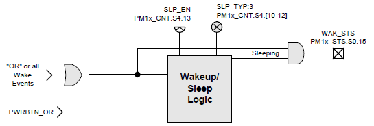
Fig. 4.10 Sleeping/Wake Logic
The logic is controlled via two bit fields: Sleep Enable (SLP_EN) and Sleep Type (SLP_TYPx). The type of sleep or soft-off state desired is programmed into the SLP_TYPx field and upon assertion of the SLP_EN the hardware will sequence the system into the defined sleeping state. OSPM gets values for the SLP_TYPx field from the \_Sx objects defined in the static definition block. If the object is missing OSPM assumes the hardware does not support that sleeping state. Prior to entering the desired sleeping state, OSPM will read the designated \_Sx object and place this value in the SLP_TYP field.
Additionally ACPI defines a fail-safe Off protocol called the “power button override,” which allows the user to initiate an Off sequence in the case where the system software is no longer able to recover the system (the system has hung). ACPI defines that this sequence be initiated by the user pressing the power button for over 4 seconds, at which point the hardware unconditionally sequences the system to the Off state. This logic is represented by the PWRBTN_OR signal coming into the sleep logic.
While in any of the sleeping states (G1), an enabled “Wake” event will cause the hardware to sequence the system back to the working state (G0). The “Wake Status” bit (WAK_STS) is provided for OSPM to “spin-on” after setting the SLP_EN/SLP_TYP bit fields. When waking from the S1 sleeping state, execution control is passed backed to OSPM immediately, whereas when waking from the S2-S4 states execution control is passed to the platform boot firmware (execution begins at the CPU’s reset vector). The WAK_STS bit provides a mechanism to separate OSPM’s sleeping and waking code during an S1 sequence. When the hardware has sequenced the system into the sleeping state (defined here as the processor is no longer able to execute instructions), any enabled wake event is allowed to set the WAK_STS bit and sequence the system back on (to the G0 state). If the system does not support the S1 sleeping state, the WAK_STS bit can always return zero.
If more than a single sleeping state is supported, then the sleeping/wake logic is required to be able to dynamically sequence between the different sleeping states. This is accomplished by waking the system; OSPM programs the new sleep state into the SLP_TYP field, and then sets the SLP_EN bit-placing the system again in the sleeping state.
4.8.2.4. Real Time Clock Alarm
If implemented, the Real Time Clock (RTC) alarm must generate a hardware wake event when in the sleeping state. The RTC can be programmed to generate an alarm. An enabled RTC alarm can be used to generate a wake event when the system is in a sleeping state. ACPI provides for additional hardware to support OSPM in determining that the RTC was the source of the wake event: the RTC_STS and RTC_EN bits. Although these bits are optional, if supported they must be implemented as described here.
If the RTC_STS and RTC_EN bits are not supported, OSPM will attempt to identify the RTC as a possible wake source; however, it might miss certain wake events. If implemented, the RTC wake feature is required to work in the following sleeping states: S1-S3. S4 wake is optional and supported through the RTC_S4 flag within the FADT (if set, then the platform supports RTC wake in the S4 state) *.
Note
* The G2/S5 “soft off” and the G3 “mechanical off” states are not sleeping states. The OS will disable the RTC_EN bit prior to entering the G2/S5 or G3 states regardless.
When the RTC generates a wake event the RTC_STS bit will be set. If the RTC_EN bit is set, an RTC hardware power management event will be generated (which will wake the system from a sleeping state, provided the battery low signal is not asserted).
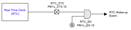
Fig. 4.11 RTC Alarm
The RTC wake event status and enable bits are an optional fixed hardware feature and a flag within the FADT (FIX_RTC) indicates if the register bits are to be used by OSPM. If the RTC wake event status and enable bits are implemented in fixed hardware, OSPM can determine if the RTC was the source of the wake event without loading the entire OS. This also gives the platform the capability of indicating an RTC wake source without consuming a GPE bit, as would be required if RTC wake was not implemented using the fixed hardware RTC feature. If the fixed hardware feature event bits are not supported, then OSPM will attempt to determine this by reading the RTC’s status field. If the platform implements the RTC fixed hardware feature, and this hardware consumes resources, the _FIX method can be used to correlate these resources with the fixed hardware. See _FIX (Fixed Register Resource Provider), for details.
OSPM supports enhancements over the existing RTC device (which only supports a 99 year date and 24-hour alarm). Optional extensions are provided for the following features:
- Day Alarm
The DAY_ALRM field points to an optional CMOS RAM location that selects the day within the month to generate an RTC alarm.
- Month Alarm
The MON_ALRM field points to an optional CMOS RAM location that selects the month within the year to generate an RTC alarm.
- Centenary Value
The CENT field points to an optional CMOS RAM location that represents the centenary value of the date (thousands and hundreds of years).
The RTC_STS bit may be set through the RTC interrupt (IRQ8 in IA-PC architecture systems). OSPM will insure that the periodic and update interrupt sources are disabled prior to sleeping. This allows the RTC’s interrupt pin to serve as the source for the RTC_STS bit generation. Note however that if the RTC interrupt pin is used for RTC_STS generation, the RTC_STS bit value may not be accurate when waking from S4. If this value is accurate when waking from S4, the platform should set the S4_RTC_STS_VALID flag, so that OSPM can utilize the RTC_STS information.
Field |
Value |
Address (Location) in RTC CMOS RAM (Must be Bank 0) |
|---|---|---|
DAY_ALRM |
Eight bit value that can represent 0x01-0x31
days in BCD or 0x01-0x1F days in binary. Bits 6
and 7 of this field are treated as Ignored by
software. The RTC is initialized such that this
field contains a “don’t care” value when the
platform firmware switches from legacy to
ACPI mode. A don’t care value can be any
unused value (not 0x1-0x31 BCD or 0x01-0x1F
hex) that the RTC reverts back to a 24 hour
alarm.
|
The DAY_ALRM field in the FADT will
contain a non-zero value that represents
an offset into the RTC’s CMOS RAM area
that contains the day alarm value. A value
of zero in the DAY_ALRM field indicates
that the day alarm feature is not
supported.
|
MON_ALRM |
Eight bit value that can represent 01-12
months in BCD or 0x01-0xC months in binary.
The RTC is initialized such that this field
contains a don’t care value when the platform
firmware switches from legacy to ACPI mode.
A “don’t care” value can be any unused value
(not 1-12 BCD or x01-xC hex) that the RTC
reverts back to a 24 hour alarm and/or 31 day
alarm).
|
The MON_ALRM field in the FADT will
contain a non-zero value that represents
an offset into the RTC’s CMOS RAM area
that contains the month alarm value. A
value of zero in the MON_ALRM field
indicates that the month alarm feature is
not supported. If the month alarm is
supported, the day alarm function must
also be supported.
|
CENTURY |
8-bit BCD or binary value. This value indicates
the thousand year and hundred year
(Centenary) variables of the date in BCD (19
for this century, 20 for the next) or binary
(x13 for this century, x14 for the next).
|
The CENTURY field in the FADT will
contain a non-zero value that represents
an offset into the RTC’s CMOS RAM area
that contains the Centenary value for the
date. A value of zero in the CENTURY field
indicates that the Centenary value is not
supported by this RTC.
|
4.8.2.5. Legacy/ACPI Select and the SCI Interrupt
As mentioned previously, power management events are generated to initiate an interrupt or hardware sequence. ACPI operating systems use the SCI interrupt handler to respond to events, while legacy systems use some type of transparent interrupt handler to respond to these events (that is, an SMI interrupt handler). ACPI-compatible hardware can choose to support both legacy and ACPI modes or just an ACPI mode. Legacy hardware is needed to support these features for non-ACPI-compatible operating systems. When the ACPI OS loads, it scans the platform firmware tables to determine that the hardware supports ACPI, and then if the it finds the SCI_EN bit reset (indicating that ACPI is not enabled), issues an ACPI activate command to the SMI handler through the SMI command port. The platform firmware acknowledges the switching to the ACPI model of power management by setting the SCI_EN bit (this bit can also be used to switch over the event mechanism as illustrated below):
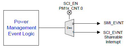
Fig. 4.12 Power Management Events to SMI/SCI Control Logic
The interrupt events (those that generate SMIs in legacy mode and SCIs in ACPI mode) are sent through a decoder controlled by the SCI_EN bit. For legacy mode this bit is reset, which routes the interrupt events to the SMI interrupt logic. For ACPI mode this bit is set, which routes interrupt events to the SCI interrupt logic. This bit always returns set for ACPI-compatible hardware that does not support a legacy power management mode (in other words, the bit is wired to read as “1” and ignore writes).
The SCI interrupt is defined to be a shareable interrupt and is connected to an OS visible interrupt that uses a shareable protocol. The FADT has an entry that indicates what interrupt the SCI interrupt is mapped to (see System Description Table Header).
If the ACPI platform supports both legacy and ACPI modes, it has a register that generates a hardware event (for example, SMI for IA-PC processors). OSPM uses this register to make the hardware switch in and out of ACPI mode. Within the FADT are three values that signify the address (SMI_CMD) of this port and the data value written to enable the ACPI state (ACPI_ENABLE), and to disable the ACPI state (ACPI_DISABLE).
To transition an ACPI/Legacy platform from the Legacy mode to the ACPI mode the following would occur:
ACPI driver checks that the SCI_EN bit is zero, and that it is in the Legacy mode.
OSPM does an OUT to the SMI_CMD port with the data in the ACPI_ENABLE field of the FADT.
OSPM polls the SCI_EN bit until it is sampled as SET.
To transition an ACPI/Legacy platform from the ACPI mode to the Legacy mode the following would occur:
ACPI driver checks that the SCI_EN bit is one, and that it is in the ACPI mode.
OSPM does an OUT to the SMI_CMD port with the data in the ACPI_DISABLE field of the FADT.
OSPM polls the SCI_EN bit until it is sampled as RESET.
Platforms that only support ACPI always return a 1 for the SCI_EN bit. In this case OSPM skips the Legacy to ACPI transition stated above.
4.8.2.6. Processor Control
The ACPI specification defines several processor controls including power state control, throttling control, and performance state control. See Processor Configuration and Control for a complete description of the processor controls.
4.8.3. Fixed Hardware Registers
The fixed hardware registers are manipulated directly by OSPM. The following sections describe fixed hardware features under the programming model. OSPM owns all the fixed hardware resource registers; these registers cannot be manipulated by AML code. Registers are accessed with any width up to its register width (byte granular).
4.8.3.1. PM1 Event Grouping
The PM1 Event Grouping has a set of bits that can be distributed between two different register blocks. This allows these registers to be partitioned between two chips, or all placed in a single chip. Although the bits can be split between the two register blocks (each register block has a unique pointer within the FADT), the bit positions are maintained. The register block with unimplemented bits (that is, those implemented in the other register block) always returns zeros, and writes have no side effects.
4.8.3.1.1. PM1 Status Registers
Register Location: <PM1a_EVT_BLK / PM1b_EVT_BLK> System I/O or Memory Space
Default Value: 00h
Attribute: Read/Write
Size: PM1_EVT_LEN / 2
The PM1 status registers contain the fixed hardware feature status bits. The bits can be split between two registers: PM1a_STS or PM1b_STS. Each register grouping can be at a different 32-bit aligned address and is pointed to by the PM1a_EVT_BLK or PM1b_EVT_BLK. The values for these pointers to the register space are found in the FADT. Accesses to the PM1 status registers are done through byte or word accesses.
For ACPI/legacy systems, when transitioning from the legacy to the G0 working state this register is cleared by platform firmware prior to setting the SCI_EN bit (and thus passing control to OSPM). For ACPI only platforms (where SCI_EN is always set), when transitioning from either the mechanical off (G3) or soft-off state to the G0 working state this register is cleared prior to entering the G0 working state.
This register contains optional features enabled or disabled within the FADT. If the FADT indicates that the feature is not supported as a fixed hardware feature, then software treats these bits as ignored.
Bit |
Name |
Description |
|---|---|---|
0 |
TMR_STS |
This is the timer carry status bit. This bit gets set any time the most significant bit of a 24/32-bit counter changes from clear to set or set to clear. While TMR_EN and TMR_STS are set, an interrupt event is raised. |
1-3 |
Reserved |
Reserved |
4 |
BM_STS |
This is the bus master status bit. This bit is set any time a system bus master requests the system bus, and can only be cleared by writing a “1” to this bit position. Notice that this bit reflects bus master activity, not CPU activity (this bit monitors any bus master that can cause an incoherent cache for a processor in the C3 state when the bus master performs a memory transaction). |
5 |
GBL_STS |
This bit is set when an SCI is generated due to the platform runtime firmware wanting the attention of the SCI handler. Platform runtime firmware will have a control bit (somewhere within its address space) that will raise an SCI and set this bit. This bit is set in response to the platform runtime firmware releasing control of the Global Lock and having seen the pending bit set. |
6-7 |
Reserved |
Reserved. These bits always return a value of zero. |
8 |
PWRBTN_STS |
This optional bit is set when the Power Button is pressed. In the system working state, while PWRBTN_EN and PWRBTN_STS are both set, an interrupt event is raised. In the sleep or soft-off state, a wake event is generated when the power button is pressed (regardless of the PWRBTN_EN bit setting). This bit is only set by hardware and can only be reset by software writing a “1” to this bit position. ACPI defines an optional mechanism for unconditional transitioning a system that has stopped working from the G0 working state into the G2 soft-off state called the power button override. If the Power Button is held active for more than four seconds, this bit is cleared by hardware and the system transitions into the G2/S5 Soft Off state (unconditionally). Support for the power button is indicated by the PWR_BUTTON flag in the FADT being reset (zero). If the PWR_BUTTON flag is set or a power button device object is present in the ACPI Namespace, then this bit field is ignored by OSPM. If the power button was the cause of the wake (from an S1-S4 state), then this bit is set prior to returning control to OSPM. |
9 |
SLPBTN_STS |
This optional bit is set when the sleep button is pressed. In the system working state, while SLPBTN_EN and SLPBTN_STS are both set, an interrupt event is raised. In the sleep or soft-off states a wake event is generated when the sleeping button is pressed and the SLPBTN_EN bit is set. This bit is only set by hardware and can only be reset by software writing a “1” to this bit position. Support for the sleep button is indicated by the SLP_BUTTON flag in the FADT being reset (zero). If the SLP_BUTTON flag is set or a sleep button device object is present in the ACPI Namespace, then this bit field is ignored by OSPM. If the sleep button was the cause of the wake (from an S1-S4 state), then this bit is set prior to returning control to OSPM. |
10 |
RTC_STS |
This optional bit is set when the RTC generates an alarm (asserts the RTC IRQ signal). Additionally, if the RTC_EN bit is set then the setting of the RTC_STS bit will generate a power management event (an SCI, SMI, or resume event). This bit is only set by hardware and can only be reset by software writing a ‘1’ to this bit position. If the RTC was the cause of the wake (from an S1-S3 state), then this bit is set prior to returning control to OSPM. If the RTC_S4 flag within the FADT is set, and the RTC was the cause of the wake from the S4 state), then this bit is set prior to returning control to OSPM. |
11 |
Ignore |
This bit field is ignored by software. |
12-14 |
Reserved |
Reserved. These bits always return a value of zero. |
14 |
PCIEXP_WAKE_STS |
This bit is optional for chipsets that implement PCI Express. This bit is set by hardware to indicate that the system woke due to a PCI Expressv wakeup event. A PCI Express wakeup event is defined as the PCI Express WAKE# pin being active , one or more of the PCI Express ports being in the beacon state, or receipt of a PCI Express PME message at a root port. This bit should only be set when one of these events causes the system to transition from a non-S0 system power state to the S0 system power state. This bit is set independent of the state of the PCIEXP_WAKE_DIS bit. Software writes a 1 to clear this bit. If the WAKE# pin is still active during the write, one or more PCI Express ports is in the beacon state or the PME message received indication has not been cleared in the root port, then the bit will remain active (i.e. all inputs to this bit are level-sensitive). Note: This bit does not itself cause a wake event or prevent entry to a sleeping state. Thus if the bit is 1 and the system is put into a sleeping state, the system will not automatically wake. |
15 |
WAK_STS |
This bit is set when the system is in the sleeping state and an enabled wake event occurs. Upon setting this bit system will transition to the working state. This bit is set by hardware and can only be cleared by software writing a “1” to this bit position. |
4.8.3.1.2. PM1Enable Registers
Register Location: <<PM1a_EVT_BLK / PM1b_EVT_BLK> + PM1_EVT_LEN / 2 System I/O or Memory Space
Default Value: 00h
Attribute: Read/Write
Size: PM1_EVT_LEN / 2
The PM1 enable registers contain the fixed hardware feature enable bits. The bits can be split between two registers: PM1a_EN or PM1b_EN. Each register grouping can be at a different 32-bit aligned address and is pointed to by the PM1a_EVT_BLK or PM1b_EVT_BLK. The values for these pointers to the register space are found in the FADT. Accesses to the PM1 Enable registers are done through byte or word accesses.
For ACPI/legacy systems, when transitioning from the legacy to the G0 working state the enables are cleared by platform firmware prior to setting the SCI_EN bit (and thus passing control to OSPM). For ACPI-only platforms (where SCI_EN is always set), when transitioning from either the mechanical off (G3) or soft-off state to the G0 working state this register is cleared prior to entering the G0 working state.
This register contains optional features enabled or disabled within the FADT. If the FADT indicates that the feature is not supported as a fixed hardware feature, then software treats the enable bits as write as zero.
Bit |
Name |
Description |
|---|---|---|
0 |
TMR_EN |
This is the timer carry interrupt enable bit. When this bit is set then an SCI event is generated anytime the TMR_STS bit is set. When this bit is reset then no interrupt is generated when the TMR_STS bit is set. |
1-4 |
Reserved |
Reserved. These bits always return a value of zero. |
5 |
GBL_EN |
The global enable bit. When both the GBL_EN bit and the GBL_STS bit are set, an SCI is raised. |
6-7 |
Reserved |
Reserved |
8 |
PWRBTN_EN |
This optional bit is used to enable the setting of the PWRBTN_STS bit to generate a power management event (SCI or wake). The PWRBTN_STS bit is set anytime the power button is asserted. The enable bit does not have to be set to enable the setting of the PWRBTN_STS bit by the assertion of the power button (see description of the power button hardware). Support for the power button is indicated by the PWR_BUTTON flag in the FADT being reset (zero). If the PWR_BUTTON flag is set or a power button device object is present in the ACPI Namespace, then this bit field is ignored by OSPM. |
9 |
SLPBTN_EN |
This optional bit is used to enable the setting of the SLPBTN_STS bit to generate a power management event (SCI or wake). The SLPBTN_STS bit is set anytime the sleep button is asserted. The enable bit does not have to be set to enable the setting of the SLPBTN_STS bit by the active assertion of the sleep button (see description of the sleep button hardware). Support for the sleep button is indicated by the SLP_BUTTON flag in the FADT being reset (zero). If the SLP_BUTTON flag is set or a sleep button device object is present in the ACPI Namespace, then this bit field is ignored by OSPM. |
10 |
RTC_EN |
This optional bit is used to enable the setting of the RTC_STS bit to generate a wake event. The RTC_STS bit is set any time the RTC generates an alarm. |
11-13 |
Reserved |
Reserved. These bits always return a value of zero. |
14 |
PCIEXP_WAKE_DIS |
This bit is optional for chipsets that implement PCI Express. This bit disables the inputs to the PCIEXP_WAKE_STS bit in the PM1 Status register from waking the system. Modification of this bit has no impact on the value of the PCIEXP_WAKE_STS bit. PCIEXP_WAKE_DIS bit. Software writes a 1 to clear this bit. If the WAKE# pin is still active during the write, one or more PCI Express ports is in the beacon state or the PME message received indication has not been cleared in the root port, then the bit will remain active (i.e. all inputs to this bit are level-sensitive). Note: This bit does not itself cause a wake event or prevent entry to a sleeping state. Thus if the bit is 1 and the system is put into a sleeping state, the system will not automatically wake. |
15 |
Reserved |
Reserved. These bits always return a value of zero. |
4.8.3.2. PM1 Control Grouping
The PM1 Control Grouping has a set of bits that can be distributed between two different registers. This allows these registers to be partitioned between two chips, or all placed in a single chip. Although the bits can be split between the two register blocks (each register block has a unique pointer within the FADT), the bit positions specified here are maintained. The register block with unimplemented bits (that is, those implemented in the other register block) returns zeros, and writes have no side effects.
4.8.3.2.1. PM1 Control Registers
Register Location: <PM1a_CNT_BLK / PM1b_CNT_BLK> System I/O or Memory Space
Default Value: 00h
Attribute: Read/Write
Size: PM1_CNT_LEN
The PM1 control registers contain the fixed hardware feature control bits. These bits can be split between two registers: PM1a_CNT or PM1b_CNT. Each register grouping can be at a different 32-bit aligned address and is pointed to by the PM1a_CNT_BLK or PM1b_CNT_BLK. The values for these pointers to the register space are found in the FADT. Accesses to PM1 control registers are accessed through byte and word accesses.
This register contains optional features enabled or disabled within the FADT. If the FADT indicates that the feature is not supported as a fixed hardware feature, then software treats these bits as ignored.
Bit |
Name |
Description |
|---|---|---|
0 |
SCI_EN |
Selects the power management event to be either an SCI or SMI interrupt for the following events. When this bit is set, then power management events will generate an SCI interrupt. When this bit is reset power management events will generate an SMI interrupt. It is the responsibility of the hardware to set or reset this bit. OSPM always preserves this bit position. |
1 |
BM_RLD |
When set, this bit allows the generation of a bus master request to cause any processor in the C3 state to transition to the C0 state. When this bit is reset, the generation of a bus master request does not affect any processor in the C3 state. |
2 |
GBL_RLS |
This write-only bit is used by the ACPI software to raise an event to the platform runtime firmware, that is, generates an SMI to pass execution control to the platform runtime firmware for IA-PC platforms. Platform runtime firmware software has a corresponding enable and status bit to control its ability to receive ACPI events (for example, BIOS_EN and BIOS_STS). The GBL_RLS bit is set by OSPM to indicate a release of the Global Lock and the setting of the pending bit in the FACS memory structure. |
8:3 |
Reserved |
Reserved. These bits are reserved by OSPM. |
9 |
Ignore |
Software ignores this bit field. |
12:10 |
SLP_TYPx |
Defines the type of sleeping or soft-off state the system enters when the SLP_EN bit is set to one. This 3-bit field defines the type of hardware sleep state the system enters when the SLP_EN bit is set. The _Sx object contains 3-bit binary values associated with the respective sleeping state (as described by the object). OSPM takes the two values from the _Sx object and programs each value into the respective SLP_TYPx field. |
13 |
SLP_EN |
This is a write-only bit and reads to it always return a zero. Setting this bit causes the system to sequence into the sleeping state associated with the SLP_TYPx fields programmed with the values from the _Sx object. |
15:14 |
Reserved |
Reserved. This field always returns zero. |
4.8.3.3. Power Management Timer (PM_TMR)
Register Location: <PM_TMR_BLK> System I/O or Memory Space
Default Value: 00h
Attribute: Read-Only
Size: 32 bits
This optional read-only register returns the current value of the power management timer (PM timer) if it is implemented on the platform. The FADT has a flag called TMR_VAL_EXT that an OEM sets to indicate a 32-bit PM timer or reset to indicate a 24-bit PM timer. When the last bit of the timer toggles the TMR_STS bit is set. This register is accessed as 32 bits.
This register contains optional features enabled or disabled within the FADT. If the FADT indicates that the feature is not supported as a fixed hardware feature, then software treats these bits as ignored.
Bit |
Name |
Description |
|---|---|---|
TMR_VAL |
23:0 |
This read-only field returns the running count of the power management timer. This is a 24-bit counter that runs off a 3.579545-MHz clock and counts while in the S0 working system state. The starting value of the timer is undefined, thus allowing the timer to be reset (or not) by any transition to the S0 state from any other state. The timer is reset (to any initial value), and then continues counting until the system’s 14.31818 MHz clock is stopped upon entering its Sx state. If the clock is restarted without a reset, then the counter will continue counting from where it stopped. |
E_TMR_VAL |
31:24 |
This read-only field returns the upper eight bits of a 32-bit power management timer. If the hardware supports a 32-bit timer, then this field will return the upper eight bits; if the hardware supports a 24-bit timer then this field returns all zeros. |
4.8.3.4. PM2 Control (PM2_CNT)
Register Location: <PM2_CNT_BLK> System I/O, System Memory, or Functional
Fixed Hardware Space
Default Value: 00h
Attribute: Read/Write
Size: PM2_CNT_LEN
This register block is naturally aligned and accessed based on its length. For ACPI 1.0 this register is byte aligned and accessed as a byte.
This register contains optional features enabled or disabled within the FADT. If the FADT indicates that the feature is not supported as a fixed hardware feature, then software treats these bits as ignored.
Bit |
Name |
Description |
|---|---|---|
0 |
ARB_DIS |
This bit is used to enable and disable the system arbiter. When this bit is CLEAR the system arbiter is enabled and the arbiter can grant the bus to other bus masters. When this bit is SET the system arbiter is disabled and the default CPU has ownership of the system. OSPM clears this bit when using the C0, C1 and C2 power states. |
>0 |
Reserved |
Reserved |
4.8.3.5. Processor Register Block (P_BLK)
This optional register block is used to control each processor in the system. There is one unique processor register block per processor in the system. For more information about controlling processors and control methods that can be used to control processors, see Processor Configuration and Control This register block is DWORD aligned and the context of this register block is not maintained across S3 or S4 sleeping states, or the S5 soft-off state.
4.8.3.5.1. Processor Control (P_CNT): 32
Register Location: Either <P_BLK>: System I/O Space
or specified by _PTC Object: System I/O, System Memory, or
Functional Fixed Hardware Space
Default Value: 00h
Attribute: Read/Write
Size: 32 bits
This register is accessed as a DWORD. The CLK_VAL field is where the duty setting of the throttling hardware is programmed as described by the DUTY_WIDTH and DUTY_OFFSET values in the FADT. Software treats all other CLK_VAL bits as ignored (those not used by the duty setting value).
Bit |
Name |
Description |
|---|---|---|
3:0 |
CLK_VAL |
Possible locations for the clock throttling value. |
4 |
THT_EN |
This bit enables clock throttling of the clock as set in the CLK_VAL field. THT_EN bit must be reset LOW when changing the CLK_VAL field (changing the duty setting). |
31:5 |
CLK_VAL |
Possible locations for the clock throttling value. |
4.8.3.5.2. Processor LVL2 Register (P_LVL2): 8
Register Location: Either <P_BLK> + 4: System I/O Space
or specified by _CST Object: System I/O, System Memory, or
Functional Fixed Hardware Space
Default Value: 00h
Attribute: Read-Only
Size: 8 bits
This register is accessed as a byte.
Bit |
Name |
Description |
|---|---|---|
7:0 |
P_LVL2 |
Reads to this register return all zeros; writes to this register have no effect. Reads to this register also generate an “enter a C2 power state” to the clock control logic. |
4.8.3.5.3. Processor LVL3 Register (P_LVL3): 8
Register Location: Either <P_BLK> + 5: System I/O Space
or specified by _CST Object: System I/O, System Memory, or
Functional Fixed Hardware Space
Default Value: 00h
Attribute: Read-Only
Size: 8 bits
This register is accessed as a byte.
Bit |
Name |
Description |
|---|---|---|
7:0 |
P_LVL3 |
Reads to this register return all zeros; writes to this register have no effect. Readsto this register also generate an “enter a C3 power state” to the clock control logic. |
4.8.3.6. Reset Register
The optional ACPI reset mechanism specifies a standard mechanism that provides a complete system reset. When implemented, this mechanism must reset the entire system. This includes processors, core logic, all buses, and all peripherals. From an OSPM perspective, asserting the reset mechanism is the logical equivalent to power cycling the system. Upon gaining control after a reset, OSPM will perform actions in like manner to a cold boot.
The reset mechanism is implemented via an 8-bit register described by RESET_REG in the FADT (always accessed via the natural alignment and size described in RESET_REG). To reset the system, software will write a value (indicated in RESET_VALUE in FADT) to the reset register. The RESET_REG field in the FADT indicates the location of the reset register.
The reset register may exist only in I/O space, Memory space, or in PCI Configuration space on a function in bus 0. Therefore, the Address_Space_ID value in RESET_REG must be set to System I/O space, System Memory space, or PCI Configuration space (with a bus number of 0). As the register is only 8 bits, Register_Bit_Width must be 8 and Register_Bit_Offset must be 0.
The system must reset immediately following the write to this register. OSPM assumes that the processor will not execute beyond the write instruction. OSPM should execute spin loops on the CPUs in the system following a write to this register.
4.8.3.7. Sleep Control and Status Registers
The optional ACPI sleep registers (SLEEP_CONTROL_REG and SLEEP_STATUS_REG) specify a standard mechanism for system sleep state entry on HW-Reduced ACPI systems. When implemented, the Sleep registers are a replacement for the SLP_TYP, SLP_EN and WAK_STS registers in the PM1_BLK. Use of these registers is at the discretion of OSPM. OSPM can decide whether to enter sleep states on the platform based on the LOW_POWER_S0_IDLE_CAPABLE flag. Even when implemented, OSPM may use other provided options for hibernate and shutdown (e.g. UEFI ResetSystem()).
The HW-reduced Sleep mechanism is implemented via two 8-bit registers described by SLEEP_CONTROL_REG and SLEEP_STATUS_REG in the FADT (always accessed via the natural alignment and size described in SLEEP_*_REG). To put the system into a sleep state, software will write the HW-reduced Sleep Type value (obtained from the \_Sx object in the DSDT) and the SLP_EN bit to the sleep control register. The OSPM then polls the WAK_STS bit of the SLEEP_STATUS_REG waiting for it to be one (1), indicating that the system has been transitioned back to the Working state.
The Sleep registers may exist only in I/O space, Memory space, or in PCI Configuration space on a function in bus 0. Therefore, the Address_Space_ID value must be set to System I/O space, SystemMemory space, or PCI Configuration space (with a bus number of 0). As the registers are only 8 bits, Register_Bit_Width must be 8 and Register_Bit_Offset must be 0.
Field Name |
Bit Length |
Bit Offset |
Description |
|---|---|---|---|
Reserved |
1 |
0 |
Reserved. This bit is reserved by OSPM. |
Ignore |
1 |
1 |
Software ignores this bit field. |
SLP_TYPx |
3 |
2 |
Defines the type of sleeping state the system enters when the SLP_EN bit is set to one. This 3-bit field defines the type of hardware sleep state the system enters when the SLP_EN bit is set. The _Sx object contains 3-bit binary values associated with the respective sleeping state (as described by the object). OSPM takes the HW-reduced Sleep Type value from the _SX object and programs it into the SLP_TYPx field. |
SLP_EN |
1 |
5 |
This is a write-only bit and reads to it always return a zero. Setting this bit causes the system to sequence into the sleeping state associated with the SLP_TYPx fields programmed with the values from the _Sx object. |
Reserved |
2 |
6 |
Reserved. This field always returns zero. |
Field Name |
Bit Length |
Bit Offset |
Description |
|---|---|---|---|
Ignore |
4 |
0 |
Software ignores this bit field. |
Reserved |
2 |
4 |
Reserved. These bits always return a value of zero. |
Ignore |
1 |
6 |
Software ignores this bit field. |
WAK_STS |
1 |
7 |
This bit is set when the system is in the sleeping state and an enabled wake event occurs. Upon setting this bit system will transition to the working state. This bit is set by hardware and can only be cleared by software writing a “1” to this bit position. |
4.8.4. Generic Hardware Registers
ACPI provides a mechanism that allows a unique piece of “value added” hardware to be described to OSPM in the ACPI Namespace. There are a number of rules to be followed when designing ACPI-compatible hardware.
Programming bits can reside in any of the defined generic hardware address spaces (system I/O, system memory, PCI configuration, embedded controller, or SMBus), but the top-level event bits are contained in the general-purpose event registers. The general-purpose event registers are pointed to by the GPE0_BLK and GPE1_BLK register blocks, and the generic hardware registers can be in any of the defined ACPI address spaces. A device’s generic hardware programming model is described through an associated object in the ACPI Namespace, which specifies the bit’s function, location, address space, and address location.
The programming model for devices is normally broken into status and control functions. Status bits are used to generate an event that allows OSPM to call a control method associated with the pending status bit. The called control method can then control the hardware by manipulating the hardware control bits or by investigating child status bits and calling their respective control methods. ACPI requires that the top level “parent” event status and enable bits reside in either the GPE0_STS or GPE1_STS registers, and “child” event status bits can reside in generic address space.
The example below illustrates some of these concepts. The top diagram shows how the logic is partitioned into two chips: a chipset and an embedded controller.
The chipset contains the interrupt logic, performs the power button (which is part of the fixed register space, and is not discussed here), the lid switch (used in portables to indicate when the clam shell lid is open or closed), and the RI# function (which can be used to wake a sleeping system).
The embedded controller chip is used to perform the AC power detect and dock/undock event logic. Additionally, the embedded controller supports some system management functions using an OS-transparent interrupt in the embedded controller (represented by the EXTSMI# signal).

Fig. 4.13 Example of General-Purpose vs. Generic Hardware Events
At the top level, the generic events in the GPEx_STS register are the:
Embedded controller interrupt, which contains two query events: one for AC detection and one for docking (the docking query event has a child interrupt status bit in the docking chip).
Ring indicate status (used for waking the system).
Lid status.
The embedded controller event status bit (EC_STS) is used to indicate that one of two query events is active.
A query event is generated when the AC# signal is asserted. The embedded controller returns a query value of 34 (any byte number can be used) upon a query command in response to this event; OSPM will then schedule for execution the control method associated with query value 34.
Another query event is for the docking chip that generates a docking event. In this case, the embedded controller will return a query value of 35 upon a query command from system software responding to an SCI from the embedded controller. OSPM will then schedule the control method associated with the query value of 35 to be executed, which services the docking event.
For each of the status bits in the GPEx_STS register, there is a corresponding enable bit in the GPEx_EN register. Notice that the child status bits do not necessarily need enable bits (see the DOCK_STS bit).
The lid logic contains a control bit to determine if its status bit is set when the LID is open (LID_POL is set and LID is set) or closed (LID_POL is clear and LID is clear). This control bit resides in generic I/O space (in this case, bit 2 of system I/O space 33h) and would be manipulated with a control method associated with the lid object.
As with fixed hardware events, OSPM will clear the status bits in the GPEx register blocks. However, AML code clears all sibling status bits in the generic hardware.
Generic hardware features are controlled by OEM supplied control methods, encoded in AML. ACPI provides both an event and control model for development of these features. The ACPI specification also provides specific control methods for notifying OSPM of certain power management and Plug and Play events. ACPI Software Programming Model provides information on the types of hardware functionality that support the different types of subsystems. The following is a list of features supported by ACPI. The list is not intended to be complete or comprehensive.
Device insertion/ejection (for example, docking, device bay, A/C adapter)
Batteries *
Platform thermal subsystem
Turning on/off power resources
Mobile lid Interface
Embedded controller
System indicators
OEM-specific wake events
Plug and Play configuration
Note
* ACPI operating systems assume the use of the Smart Battery System Implementers Forum defined standard for batteries, called the “Smart Battery Specification” (SBS). ACPI provides a set of control methods for use by OEMs that use a proprietary “control method” battery interface.
4.8.4.1. General-Purpose Event Register Blocks
ACPI supports up to two general-purpose register blocks as described in the FADT (see ACPI Software Programming Model ), and an arbitrary number of additional GPE blocks described as devices within the ACPI namespace. Each register block contains two registers: an enable and a status register. Each register block is 32-bit aligned. Each register in the block is accessed as a byte. It is up to the specific design to determine if these bits retain their context across sleeping or soft-off states. If they lose their context across a sleeping or soft-off state, then platform boot firmware resets the respective enable bit prior to passing control to the OS upon waking.
4.8.4.1.1. General-Purpose Event 0 Register Block
This register block consists of two registers: The GPE0_STS and the GPE0_EN registers. Each register’s length is defined to be half the length of the GPE0 register block, and is described in the ACPI FADT’s GPE0_BLK and GPE0_BLK_LEN operators. OSPM owns the general-purpose event resources and these bits are only manipulated by OSPM; AML code cannot access the general-purpose event registers.
It is envisioned that chipsets will contain GPE event registers that provide GPE input pins for various events.
The platform designer would then wire the GPEs to the various value-added event hardware and the AML code would describe to OSPM how to utilize these events. As such, there will be the case where a platform has GPE events that are not wired to anything (they are present in the chip set), but are not utilized by the platform and have no associated AML code. In such, cases these event pins are to be tied inactive such that the corresponding SCI status bit in the GPE register is not set by a floating input pin.
4.8.4.1.1.1. General-Purpose Event 0 Status Register
Register Location: <GPE0_STS> System I/O or System Memory Space
Default Value: 00h
Attribute: Read/Write
Size: GPE0_BLK_LEN/2
The general-purpose event 0 status register contains the general-purpose event status bits in bank zero of the general-purpose registers. Each available status bit in this register corresponds to the bit with the same bit position in the GPE0_EN register. Each available status bit in this register is set when the event is active, and can only be cleared by software writing a “1” to its respective bit position. For the general-purpose event registers, unimplemented bits are ignored by OSPM.
Each status bit can optionally wake the system if asserted when the system is in a sleeping state with its respective enable bit set. OSPM accesses GPE registers through byte accesses (regardless of their length).
4.8.4.1.1.2. General-Purpose Event 0 Enable Register
Register Location: <GPE0_EN> System I/O or System Memory Space
Default Value: 00h
Attribute: Read/Write
Size: GPE0_BLK_LEN/2
The general-purpose event 0 enable register contains the general-purpose event enable bits. Each available enable bit in this register corresponds to the bit with the same bit position in the GPE0_STS register. The enable bits work similarly to how the enable bits in the fixed-event registers are defined: When the enable bit is set, then a set status bit in the corresponding status bit will generate an SCI bit. OSPM accesses GPE registers through byte accesses (regardless of their length).
4.8.4.1.2. General-Purpose Event 1 Register Block
This register block consists of two registers: The GPE1_STS and the GPE1_EN registers. Each register’s length is defined to be half the length of the GPE1 register block, and is described in the ACPI FADT’s GPE1_BLK and GPE1_BLK_LEN operators.
4.8.4.1.2.1. General-Purpose Event 1 Status Register
Register Location: <GPE1_STS> System I/O or System Memory Space
Default Value: 00h
Attribute: Read/Write
Size: GPE1_BLK_LEN/2
The general -purpose event 1 status register contains the general-purpose event status bits. Each available status bit in this register corresponds to the bit with the same bit position in the GPE1_EN register. Each available status bit in this register is set when the event is active, and can only be cleared by software writing a “1” to its respective bit position. For the general-purpose event registers, unimplemented bits are ignored by the operating system.
Each status bit can optionally wake the system if asserted when the system is in a sleeping state with its respective enable bit set.
OSPM accesses GPE registers through byte accesses (regardless of their length).
4.8.4.1.2.2. General-Purpose Event 1 Enable Register
Register Location: <GPE1_EN> System I/O or System Memory Space
Default Value: 00h
Attribute: Read/Write
Size: GPE1_BLK_LEN/2
The general-purpose event 1 enable register contains the general-purpose event enable. Each available enable bit in this register corresponds to the bit with the same bit position in the GPE1_STS register. The enable bits work similarly to how the enable bits in the fixed-event registers are defined: When the enable bit is set, a set status bit in the corresponding status bit will generate an SCI bit.
OSPM accesses GPE registers through byte accesses (regardless of their length).
4.8.4.2. Example Generic Devices
This section points out generic devices with specific ACPI driver support.
4.8.4.2.1. Lid Switch
The Lid switch is an optional feature present in most “clam shell” style mobile computers. It can be used by the OS as policy input for sleeping the system, or for waking the system from a sleeping state. If used, then the OEM needs to define the lid switch as a device with an _HID object value of “PNP0C0D”, which identifies this device as the lid switch to OSPM. The Lid device needs to contain a control method that returns its status. The Lid event handler AML code reconfigures the lid hardware (if it needs to) to generate an event in the other direction, clear the status, and then notify OSPM of the event.
Example hardware and ASL code is shown below for such a design.

Fig. 4.14 Example Generic Address Space Lid Switch Logic
This logic will set the Lid status bit when the button is pressed or released (depending on the LID_POL bit).
The ASL code below defines the following:
An operational region where the lid polarity resides in address space System address space in registers 0x201.
A field operator to allow AML code to access this bit: Polarity control bit (LID_POL) is called LPOL and is accessed at 0x201.0.
A device named \_SB.LID with the following:
A Plug and Play identifier “PNP0C0D” that associates OSPM with this object.
Defines an object that specifies a change in the lid’s status bit can wake the system from the S4 sleep state and from all higher sleep states (S1, S2, or S3).
The lid switch event handler that does the following:
Defines the lid status bit (LID_STS) as a child of the general-purpose event 0 register bit 1.
Defines the event handler for the lid (only event handler on this status bit) that does the following:
Flips the polarity of the LPOL bit (to cause the event to be generated on the opposite condition).
Generates a notify to the OS that does the following:
Passes the \_SB.LID object.
Indicates a device specific event (notify value 0x80).
// Define a Lid switch
OperationRegion (\PHO, SystemIO, 0x201, 0x1)
Field (\PHO, ByteAcc, NoLock, Preserve)
{
     LPOL, 1                    // Lid polarity control bit
}

Device (\_SB.LID)
{
    Name (_HID, EISAID ("PNP0C0D"))
    Method (_LID)
    {
       Return(LPOL)
    }
    Name (_PRW, Package (2){
        1,                      // bit 1 of GPE to enable Lid wakeup
        0x04})                  // can wakeup from S4 state
}

Scope(\_GPE)
{
    Method(_L01)                // uses bit 1 of GP0_STS register
    {
        LPOL ~= LPOL            // Flip the lid polarity bit
        Notify (\_SB.LID, 0x80) // Notify OS of event
    }
}
4.8.4.2.2. Embedded Controller
ACPI provides a standard interface that enables AML code to define and access generic logic in “embedded controller space.” This supports current computer models where much of the value added hardware is contained within the embedded controller while allowing the AML code to access this hardware in an abstracted fashion.
The embedded controller is defined as a device and must contain a set number of control methods:
_HID with a value of PNP0C09 to associate this device with the ACPI’s embedded controller’s driver.
_CRS to return the resources being consumed by the embedded controller.
_GPE that returns the general-purpose event bit that this embedded controller is wired to.
Additionally the embedded controller can support up to 255 generic events per embedded controller, referred to as query events. These query event handles are defined within the embedded controller’s device as control methods. An example of defining an embedded controller device is shown below:
Device(EC0) {
    // PnP ID
    Name(_HID, EISAID("PNP0C09"))
    // Returns the "Current Resources" of EC
    Name (_CRS, ResourceTemplate()
    {
        IO(Decode16, 0x62, 0x62, 0, 1)
        IO(Decode16, 0x66, 0x66, 0, 1)
    })

    // Indicate that the EC SCI is bit 0 of the GP_STS register
    Name (_GPE, 0)          // embedded controller is wired to bit 0 of GPE
    OperationRegion (\EC0, EmbeddedControl, 0, 0xFF)
    Field (EC0, ByteAcc, Lock, Preserve)
    {
    // Field units of EC0
    }

    // Query methods
    Method(_Q00)
    { ...  }
    Method(_QFF)
    { ...  }
}
For more information on the embedded controller, see ACPI Embedded Controller Interface Specification
4.8.4.2.3. Fan
ACPI has a device driver to control fans (active cooling devices) in platforms. A fan is defined as a device with the Plug and Play ID of “PNP0C0B.” It should then contain a list power resources used to control the fan.
For more information, see ACPI-Defined Devices and Device-Specific Objects.