18. ACPI Platform Error Interfaces (APEI)
This section describes the ACPI Platform Error Interfaces (APEI), which provide a means for a computer platform to convey error information to OSPM. APEI extends existing hardware error reporting mechanisms and brings them together as components of a coherent hardware error infrastructure. APEI takes advantage of the additional hardware error information available in today’s hardware devices, and integrates much more closely with the system firmware.
As a result, APEI provides the following benefits:
Allows for more extensive error data to be made available in a standard error record format for determining the root cause of hardware errors.
Is extensible, so that as hardware vendors add new and better hardware error reporting mechanisms to their devices, APEI allows the platform and the OSPM to gracefully accommodate the new mechanisms.
This provides information to help system designers understand basic issues about hardware errors, the relationship between the firmware and OSPM, and information about error handling and the APEI architecture components.
APEI consists of four separate tables:
Error Record Serialization Table (ERST)
Boot Error Record Table (BERT)
Hardware Error Source Table (HEST)
Error Injection Table (EINJ)
18.1. Hardware Errors and Error Sources
A hardware error is a recorded event related to a malfunction of a hardware component in a computer platform. The hardware components contain error detection mechanisms that detect when a hardware error condition exists. Hardware errors can be classified as either corrected errors or uncorrected errors as follows:
A corrected error is a hardware error condition that has been corrected by the hardware or by the firmware by the time the OSPM is notified about the existence of the error condition.
An uncorrected error is a hardware error condition that cannot be corrected by the hardware or by the firmware. Uncorrected errors are either fatal or non-fatal.
A fatal hardware error is an uncorrected or uncontained error condition that is determined to be unrecoverable by the hardware. When a fatal uncorrected error occurs, the system is restarted to prevent propagation of the error.
A non-fatal hardware error is an uncorrected error condition from which OSPM can attempt recovery by trying to correct the error. These are also referred to as correctable or recoverable errors.
Central to APEI is the concept of a hardware error source. A hardware error source is any hardware unit that alerts OSPM to the presence of an error condition. Examples of hardware error sources include the following:
Processor machine check exception (for example, MC#)
Chipset error message signals (for example, SCI, SMI, SERR#, MCERR#)
I/O bus error reporting (for example, PCI Express root port error interrupt)
I/O device errors
A single hardware error source might handle aggregate error reporting for more than one type of hardware error condition. For example, a processor’s machine check exception typically reports processor errors, cache and memory errors, and system bus errors.
A hardware error source is typically represented by the following:
One or more hardware error status registers.
One or more hardware error configuration or control registers.
A signaling mechanism to alert OSPM to the existence of an error condition.
In some situations, there is not an explicit signaling mechanism and OSPM must poll the error status registers to test for an error condition. However, polling can only be used for corrected error conditions since uncorrected errors require immediate attention by OSPM.
18.2. Relationship between OSPM and System Firmware
Both OSPM and system firmware play important roles in hardware error handling. APEI improves the methods by which both of these can contribute to the task of hardware error handling in a complementary fashion. APEI allows the hardware platform vendor to determine whether the firmware or OSPM will own key hardware error resources. APEI also allows the firmware to pass control of hardware error resources to OSPM when appropriate.
18.3. Error Source Discovery
Platforms enumerate error sources to OSPM via a set of tables that describe the error sources. OSPM may also support non-ACPI enumerated error sources such as: Machine Check Exception, Corrected Machine Check, NMI, PCI Express AER, and on Itanium™ Processor Family (IPF) platforms the INIT error source. Non-ACPI error sources are not described by this specification.
During initialization, OSPM examines the tables and uses this information to establish the necessary error handlers that are responsible for processing error notifications from the platform.
18.3.1. Boot Error Source
Under normal circumstances, when a hardware error occurs, the error handler receives control and processes the error. This gives OSPM a chance to process the error condition, report it, and optionally attempt recovery. In some cases, the system is unable to process an error. For example, system firmware or a management controller may choose to reset the system or the system might experience an uncontrolled crash or reset.
The boot error source is used to report unhandled errors that occurred in a previous boot. This mechanism is described in the BERT table. The boot error source is reported as a ‘one-time polled’ type error source. OSPM queries the boot error source during boot for any existing boot error records. The platform will report the error condition to OSPM via a Common Platform Error Record (CPER) compliant error record. The CPER format is described in the appendices of the UEFI Specification.
The following table describes the format for the Boot Error Record Table (BERT).
Field |
Byte length |
Byte offset |
Description |
|---|---|---|---|
Header Signature |
4 |
0 |
‘BERT’. Signature for the Boot Error Record Table. |
Length |
4 |
4 |
Length, in bytes, of BERT. |
Revision |
1 |
8 |
1 |
Checksum |
1 |
9 |
Entire table must sum to zero. |
OEMID |
6 |
10 |
OEM ID. |
OEM Table ID |
8 |
16 |
The manufacturer model ID. |
OEM Revision |
4 |
24 |
OEM revision of the BERT for the supplied OEM table ID. |
Creator ID |
4 |
28 |
Vendor ID of the utility that created the table. |
Creator Revision |
4 |
32 |
Revision of the utility that created the table. |
Boot Error Region Length |
4 |
36 |
The length in bytes of the boot error region. |
Boot Error Region |
8 |
40 |
64-bit physical address of the Boot Error Region. |
The Boot Error Region is a range of addressable memory that OSPM can access during initialization, to determine if an unhandled error condition occurred. System firmware must report this memory range as firmware reserved. The format of the Boot Error Region follows that of an Error Status Block, as defined in the Generic Hardware Error Source Structure. The format of the error status block is described by the Generic Error Status Block table.
For details of some of the fields listed in the Generic Error Data Entry table, please see the Section Descriptors definitions in the the UEFI Specification appendices, under the description of the Common Platform Error Record.
18.3.2. ACPI Error Source
The hardware error source describes a standardized mechanism platforms may use to describe their error sources. Use of this interface is the preferred way for platforms to describe their error sources as it is platform and processor-architecture independent and allows the platform to describe the operational parameters associated with error sources.
This mechanism allows for the platform to describe error sources in detail; communicating operational parameters (i.e. severity levels, masking bits, and threshold values) to OSPM as necessary. It also allows the platform to report error sources for which OSPM would typically not implement support (for example, chipset-specific error registers).
The Hardware Error Source Table (HEST) provides the platform firmware a way to describe a system’s hardware error sources to OSPM. The HEST format is shown in the following table.
Field |
Byte length |
Byte offset |
Description |
|---|---|---|---|
Header Signature |
4 |
0 |
“HEST”. Signature for the Hardware Error Source Table. |
Length |
4 |
4 |
Length, in bytes, of entire HEST. Entire table must be contiguous. |
Revision |
1 |
8 |
2 |
Checksum |
1 |
9 |
Entire table must sum to zero. |
OEMID |
6 |
10 |
OEM ID. |
OEM Table ID |
8 |
16 |
The manufacturer model ID. |
OEM Revision |
4 |
24 |
OEM revision of the HEST for the supplied OEM table ID. |
Creator ID |
4 |
28 |
Vendor ID of the utility that created the table. |
Creator Revision |
4 |
32 |
Revision of the utility that created the table. |
Error Source Count |
4 |
36 |
The number of error source descriptors. |
Error Source Structure[n] |
40 |
A series of Error Source Descriptor Entries. |
Note
Error source types 3, 4, and 5 are reserved for legacy reasons and must not be used.
Note
Starting with revision 2 of HEST, the Error Source Structures must be sorted in Type ascending order for Error Source Structure Types of less than 12.
Note
Beginning with error source type 12 and onward, each Error Source Structure must use the standard Error Source Structure Header as defined in Section 18.3.2.11.
The following sections detail each of the specific error source descriptors.
18.3.2.1. IA-32 Architecture Machine Check Exception
Processors implementing the IA-32 Instruction Set Architecture employ a machine check exception mechanism to alert OSPM to the presence of an uncorrected hardware error condition. The information in this table is used by OSPM to configure the machine check exception mechanism for each processor in the system.
Only one entry of this type is permitted in the HEST. OSPM applies the information specified in this entry to all processors.
Field |
Byte Length |
Byte Offset |
Description |
|---|---|---|---|
Type |
2 |
0 |
0 - IA-32 Architecture Machine Check Exception Structure. |
Source Id |
2 |
2 |
This value serves to uniquely identify this error source against other error sources reported by the platform. |
Reserved |
2 |
4 |
Reserved. |
Flags |
1 |
6 |
Bit [0] - FIRMWARE_FIRST: If set, this bit indicates to the OSPM that the interrupt handler from system firmware will run first for this error source.
Bit [2] - GHES_ASSIST: If set, this bit indicates that although OSPM is responsible for directly handling the error (as expected when FIRMWARE_FIRST is not set), system firmware may report additional information in the context of the error reported by hardware. The additional information is reported in a Generic Hardware Error Source structure with a matching Related Source ID. See Section 18.7, GHES_ASSIST Error Reporting. NOTE: If FIRMWARE_FIRST is set, this bit is reserved.
All other bits are reserved.
|
Enabled |
1 |
7 |
Specifies whether MCE is to be enabled. If set to 1, this field indicates this error source is to be enabled. If set to 0, this field indicates that the error source is not to be enabled. |
Number of Records To Pre-allocate |
4 |
8 |
Indicates the number of error records to pre-allocate for this error source. |
Max Sections Per Record |
4 |
12 |
Indicates the maximum number of error sections included in an error record created as a result of an error reported by this error source. |
Global Capability Init Data |
8 |
16 |
Indicates the value of the machine check global capability register. |
Global Control Init Data |
8 |
24 |
Indicates the value to be written to the machine check global control register. |
Number Of Hardware Banks |
1 |
32 |
Indicates the number of hardware error reporting banks. |
Reserved |
7 |
33 |
Reserved. |
Machine Check Bank Structure[n] |
40 |
A list of Machine Check Bank structures defined in the IA-32 Architecture Machine Check Bank Structure |
18.3.2.1.1. IA-32 Architecture Machine Check Bank Structure
This table describes the attributes of a specific IA-32 architecture machine check hardware error bank.
Field |
Byte Length |
Byte Offset |
Description |
|---|---|---|---|
Bank Number |
1 |
0 |
Zero-based index identifies the machine check error bank. |
Clear Status On Initialization |
1 |
1 |
If set, indicates the status information in this machine check bank is to be cleared during system initialization as follows: 0 - Clear 1 - Don’t clear |
Status Data Format |
1 |
2 |
Identifies the format of the data in the status register:
0 - IA-32 MCA
1 - Intel® 64 MCA
2 - AMD64MCA All other values are reserved
|
Reserved |
1 |
3 |
Reserved. |
Control Register MSR Address |
4 |
4 |
Address of the hardware bank’s control MSR. Ignored if zero. |
Control Init Data |
8 |
8 |
This is the value the OSPM will program into the machine check bank’s control register. |
Status Register MSR Address |
4 |
16 |
Address of the hardware bank’s MCi_STAT MSR. Ignored if zero. |
Address Register MSR Address |
4 |
20 |
Address of the hardware bank’s MCi_ADDR MSR. Ignored if zero. |
Misc Register MSR Address |
4 |
24 |
Address of the hardware bank’s MCi_MISC MSR. Ignored if zero. |
18.3.2.2. IA-32 Architecture Corrected Machine Check
Processors implementing the IA-32 Instruction Set Architecture may report corrected processor errors to OSPM. The information in this table allows platform firmware to communicate key parameters of the corrected processor error reporting mechanism to OSPM, including whether CMC processing should be enabled.
Only one entry of this type is permitted in the HEST. OSPM applies the information specified in this entry to all processors.
Field |
Byte Length |
Byte Offset |
Description |
|---|---|---|---|
Type |
2 |
0 |
1 - IA-32 Architecture Corrected Machine Check Structure. |
Source Id |
2 |
2 |
Uniquely identifies the error source. |
Reserved |
2 |
4 |
Reserved |
Flags |
1 |
6 |
Bit [0] - FIRMWARE_FIRST: If set, this bit indicates to the OSPM that the interrupt handler from system firmware will run first for this error source.
Bit [2] - GHES_ASSIST: If set, this bit indicates that although OSPM is responsible for directly handling the error (as expected when FIRMWARE_FIRST is not set), system firmware may report additional information in the context of the error reported by hardware. The additional information is reported in a Generic Hardware Error Source structure with a matching Related Source ID. See Section 18.7, GHES_ASSIST Error Reporting. NOTE: If FIRMWARE_FIRST is set, this bit is reserved.
All other bits must be set to zero.
|
Enabled |
1 |
7 |
If the field value is 1, indicates this error source is to be enabled.
If the field value is 0, indicates that the error source is not to be enabled.
If FIRMWARE_FIRST is set in the flags field, the Enabled field is ignored by OSPM.
|
Number of Records To Pre-allocate |
4 |
8 |
Indicates the number of error records to pre-allocate for this error source. Must be >= 1. |
Max Sections Per Record |
4 |
12 |
Indicates the maximum number of error sections included in an error record created as a result of an error reported by this error source. Must be >= 1. |
Notification Structure |
28 |
16 |
Hardware Error Notification Structure as defined in Hardware Error Notification Structure. |
Number Of Hardware Banks |
1 |
44 |
The number of hardware error reporting banks. |
Reserved |
3 |
45 |
Reserved. |
Machine Check Bank Structure[n] |
48 |
A list of Machine Check Bank structures defined in IA-32 Architecture Machine Check Bank Structure. |
18.3.2.3. IA-32 Architecture Non-Maskable Interrupt
Uncorrected platform errors are typically reported using the Non-Maskable Interrupt (NMI) vector (for example, INT 2). This table allows platform firmware to communicate parameters regarding the configuration and handling of NMI error conditions.
Only one entry of this type is permitted in the HEST.
Field |
Byte Length |
Byte Offset |
Description |
|---|---|---|---|
Type |
2 |
0 |
2 - IA-32 Architecture NMI Structure. |
Source Id |
2 |
2 |
Uniquely identifies this error source. |
Reserved |
4 |
4 |
Must be zero. |
Number of Records To Pre-allocate |
4 |
8 |
Indicates number of error records to pre-allocate for this error source. Must be >= 1. |
Max Sections Per Record |
4 |
12 |
Indicates maximum number of error sections included in an error record created as a result of an error reported by this error source. Must be >= 1. |
Max Raw Data Length |
4 |
16 |
The size in bytes of the NMI error data. |
18.3.2.4. PCI Express Root Port AER Structure
PCI Express (PCIe) root ports may implement PCIe Advanced Error Reporting (AER) support. This table contains information platform firmware supplies to OSPM for configuring AER support on a given root port.
The HEST may contain one entry of this type for each PCI Express root port if none of the entries has the GLOBAL flag set. If the GLOBAL flag is set, there may only be one entry of this type and the information contained in that entry is applied to all PCIe root ports.
Field |
Byte Length |
Byte Offset |
Description |
|---|---|---|---|
Type |
2 |
0 |
6 - AER Root Port. |
Source Id |
2 |
2 |
Uniquely identifies the error source. |
Reserved |
2 |
4 |
Reserved. |
Flags |
1 |
6 |
Bit [0] - FIRMWARE_FIRST: If set, this bit indicates to the OSPM that the interrupt handler from system firmware will run first for this error source. This flag does not grant nor deny access to AER registers. OSPM should evaluate _OSC for PCI hierarchies to determine AER register ownership.
Bit [1] - GLOBAL: If set, indicates that the settings contained in this structure apply globally to all PCI Express Devices.
All other bits must be set to zero.
|
Enabled |
1 |
7 |
If the field value is 1, indicates this error source is to be enabled. If the field value is 0, indicates that the error source is not to be enabled. If FIRMWARE_FIRST is set in the flags field, the Enabled field is ignored by the OSPM. |
Number of Records To Pre-allocate |
4 |
8 |
Indicates the number error records to pre-allocate for this error source. Must be >= 1. |
Max Sections Per Record |
4 |
12 |
Indicates the maximum number of error sections included in an error record created as a result of an error reported by this error source. Must be >= 1. |
Bus |
4 |
16 |
Identifies the PCI Bus and Segment of the root port.
The Bus is encoded in bits [7:0].
For systems that expose multiple PCI segment groups, the segment number is encoded in bits [23:8], and bits [31-24] must be zero.
For systems that do not expose multiple PCI segment groups, bits [31:8] must be zero.
If the GLOBAL flag is specified, this field is ignored.
|
Device |
2 |
20 |
Identifies the PCI Device Number of the root port. If the GLOBAL flag is specified, this field is ignored. |
Function |
2 |
22 |
Identifies the PCI Function number of the root port. If the GLOBAL flag is specified, this field is ignored. |
Device Control |
2 |
24 |
Device control bits with which to initialize the device. |
Reserved |
2 |
26 |
Must be zero. |
Uncorrectable Error Mask |
4 |
28 |
Value to write to the root port’s Uncorrectable Error Mask register. |
Uncorrectable Error Severity |
4 |
32 |
Value to write to the root port’s Uncorrectable Error Severity register. |
Correctable Error Mask |
4 |
36 |
Value to write to the root port’s Correctable Error Mask register. |
Advanced Error Capabilities and Control |
4 |
40 |
Value to write to the root port’s Advanced Error Capabilities and Control Register. |
Root Error Command |
4 |
44 |
Value to write to the root port’s Root Error Command Register. |
Note
For PCI Express Advanced Error Reporting (AER) resources, ownership and control of AER registers are determined by the evaluation of the PCI _OSC() method as described in the most current revision of the PCI Firmware Specification. The FIRMWARE_FIRST bit in the Flags Field does not serve to grant, nor deny, access to the AER registers within the PCI Express device(s) that are described by the structure.
18.3.2.5. PCI Express Device AER Structure
PCI Express devices may implement AER support. This table contains information platform firmware supplies to OSPM for configuring AER support on a given PCI Express device.
The HEST may contain one entry of this type for each PCI Express endpoint device if none of the entries has the GLOBAL flag set. If the GLOBAL flag is set, there may only be one entry of this type and the information contained in that entry will be applied to all PCI Express endpoint devices.
Field |
Byte Length |
Byte Offset |
Description |
|---|---|---|---|
Type |
2 |
0 |
7 - AER Endpoint. |
Source Id |
2 |
2 |
Uniquely identifies the error source. |
Reserved |
2 |
4 |
Reserved. |
Flags |
1 |
6 |
Bit [0] - FIRMWARE_FIRST: If set, this bit indicates to the OSPM that the interrupt handler from system firmware will run first for this error source. This flag does not grant nor deny access to AER registers. OSPM should evaluate _OSC for PCI hierarchies to determine AER register ownership.
Bit [1] - GLOBAL: If set, indicates that the settings contained in this structure apply globally to all PCI Express Devices.
All other bits must be set to zero.
|
Enabled |
1 |
7 |
If the field value is 1, indicates this error source is to be enabled.
If the field value is 0, indicates that the error source is not to be enabled.
If FIRMWARE_FIRST is set in the flags field, the Enabled field is ignored by the OSPM.
|
Number of Records To Pre-allocate |
4 |
8 |
Indicates the number of error records to pre-allocate for this error source. Must be >= 1. |
Max Sections Per Record |
4 |
12 |
Indicates the maximum number of error sections included in an error record created as a result of an error reported by this error source. Must be >= 1. |
Bus |
4 |
16 |
Identifies the PCI Bus and Segment of the device.
The Bus is encoded in bits [7:0].
For systems that expose multiple PCI segment groups, the segment number is encoded in bits [23:8], and bits [31:24] must be zero.
For systems that do not expose multiple PCI segment groups, bits 8-31 must be zero.
If the GLOBAL flag is specified, this field is ignored.
|
Device |
2 |
20 |
Identifies the PCI Device Number of the device. If the GLOBAL flag is specified, this field is ignored. |
Function |
2 |
22 |
Identifies the PCI Function Number of the device. If the GLOBAL flag is specified, this field is ignored. |
Device Control |
2 |
24 |
Device control bits with which to initialize the device. |
Reserved |
2 |
26 |
Must be zero. |
Uncorrectable Error Mask |
4 |
28 |
Value to write to the root port’s Uncorrectable Error Mask register. |
Uncorrectable Error Severity |
4 |
32 |
Value to write to the root port’s Uncorrectable Error Severity register. |
Correctable Error Mask |
4 |
36 |
Value to write to the root port’s Correctable Error Mask register. |
Advanced Error Capabilities and Control |
4 |
40 |
Value to write to the root port’s Advanced Error Capabilities and Control Register. |
Note
For PCI Express Advanced Error Reporting (AER) resources, ownership and control of AER registers are determined by the evaluation of the PCI _OSC() method as described in the most current revision of the PCI Firmware Specification. The FIRMWARE_FIRST bit in the Flags Field does not serve to grant, nor deny, access to the AER registers within the PCI Express device(s) that are described by the structure.
18.3.2.6. PCI Express/PCI-X Bridge AER Structure
PCI Express/PCI-X bridges that implement AER support implement fields that control the behavior how errors are reported across the bridge.
The HEST may contain one entry of this type for each PCI Express/PCI-X bridges if none of the entries has the GLOBAL flag set. If the GLOBAL flag is set, there may only be one entry of this type and the information contained in that entry will be applied to all PCI Express/ PCI-X bridges.
Field |
Byte Length |
Byte Offset |
Description |
|---|---|---|---|
Type |
2 |
0 |
8 - AER Bridge. |
Source Id |
2 |
2 |
Uniquely identifies the error source. |
Reserved |
2 |
4 |
Reserved. |
Flags |
1 |
6 |
Bit [0] - FIRMWARE_FIRST: If set, this bit indicates to the OSPM that the interrupt handler from system firmware will run first for this error source. This flag does not grant nor deny access to AER registers. OSPM should evaluate _OSC for PCI hierarchies to determine AER register ownership.
Bit [1] - GLOBAL: If set, indicates that the settings contained in this structure apply globally to all PCI Express Devices.
All other bits must be set to zero.
|
Enabled |
1 |
7 |
If the field value is 1, indicates this error source is to be enabled.
If the field value is 0, indicates that the error source is not to be enabled.
If FIRMWARE_FIRST is set in the flags field, the Enabled field is ignored by the OSPM.
|
Number of Records To Pre-allocate |
4 |
8 |
Indicates the number of error records to pre-allocate for this error source. Must be >= 1. |
Max Sections Per Record |
4 |
12 |
Indicates the maximum number of error sections included in an error record created as a result of an error reported by this error source. Must be >= 1. |
Bus |
4 |
16 |
Identifies the PCI Bus and Segment of the bridge.
The Bus is encoded in bits [7:0].
For systems that expose multiple PCI segment groups, the segment number is encoded in bits [23:8], and bits [31:24] must be zero.
For systems that do not expose multiple PCI segment groups, bits 8-31 must be zero. If the GLOBAL flag is specified, this field is ignored.
|
Device |
2 |
20 |
Identifies the PCI device number of the bridge. If the GLOBAL flag is specified, this field is ignored. |
Function |
2 |
22 |
Identifies the PCI function number of the bridge. If the GLOBAL flag is specified, this field is ignored. |
Device Control |
2 |
24 |
Device control bits with which to initialize the device. |
Reserved |
2 |
26 |
This value must be zero. |
Uncorrectable Error Mask |
4 |
28 |
Value to write to the bridge’s Uncorrectable Error Mask register. |
Uncorrectable Error Severity |
4 |
32 |
Value to write to the bridge’s Uncorrectable Error Severity register. |
Correctable Error Mask |
4 |
36 |
Value to write to the bridge’s Correctable Error Mask register. |
Advanced Error Capabilities and Control |
4 |
40 |
Value to write to the bridge’s Advanced Error Capabilities and Control Register. |
Secondary Uncorrectable Error Mask |
4 |
44 |
Value to write to the bridge’s secondary uncorrectable error mask register. |
Secondary Uncorrectable Error Severity |
4 |
48 |
Value to write to the bridge’s secondary uncorrectable error severity register. |
Secondary Advanced Capabilities and Control |
4 |
52 |
Value to write to the bridge’s secondary advanced capabilities and control register. |
Note
For PCI Express Advanced Error Reporting (AER) resources, ownership and control of AER registers are determined by the evaluation of the PCI _OSC() method as described in the most current revision of the PCI Firmware Specification. The FIRMWARE_FIRST bit in the Flags Field does not serve to grant, nor deny, access to the AER registers within the PCI Express device(s) that are described by the structure.
18.3.2.7. Generic Hardware Error Source
The platform may describe a generic hardware error source to OSPM using the Generic Hardware Error Source structure. A generic hardware error source is an error source that either notifies OSPM of the presence of an error using a non-standard notification mechanism or reports error information that is encoded in a non-standard format.
Using the information in a Generic Hardware Error Source structure, OSPM configures an error handler to read the error data from an error status block - a memory range set aside by the platform for recording error status information.
As the generic hardware error source is non-standard, OSPM does not implement built-in support for configuration and control operations. The error source must be configured by system firmware during boot.
Some platforms may describe multiple Generic Hardware Error Source structures with different notification types, as defined in Table 18.10. For example, a platform may describe one error source for the handling of synchronous errors (e.g. MCE or SEA), and a second source for handling asynchronous errors (e.g. SCI or External Interrupt).
Field |
Byte Length |
Byte Offset |
Description |
|---|---|---|---|
Type |
2 |
0 |
9 - Generic Hardware Error Source Structure. |
Source Id |
2 |
2 |
Uniquely identify the error source. |
Related Source ID |
2 |
4 |
This field represents the Source ID of an alternate error source for which the platform:
(a) Requires Firmware-First handling (FIMWARE_FIRST flag is set on alternate error source). See Section 18.4.
(b) Provides additional information in the context of an error reported by hardware (GHES_ASSIST flag is set on alternate error source). See Section 18.7.
If this generic error source does not represent an alternate source, this field must be set to 0xFFFF.
|
Flags |
1 |
6 |
Reserved. |
Enabled |
1 |
7 |
If the field value is 1, indicates this error source is to be enabled.
If the field value is 0, indicates that the error source is not to be enabled.
|
Number of Records To Pre-allocate |
4 |
8 |
Indicates the number of error records to pre-allocate for this error source. Must be >= 1. |
Max Sections Per Record |
4 |
12 |
Indicates the maximum number of error sections included in an error record created as a result of an error reported by this error source. Must be >= 1. |
Max Raw Data Length |
4 |
16 |
Indicates the size in bytes of the error data recorded by this error source. |
Error Status Address |
12 |
20 |
Generic Address Structure as defined in Section 5.2.3.2. This field specifies the location of a register that contains the physical address of a block of memory that holds the error status data for this error source. This memory range must reside in firmware reserved memory. OSPM maps this range into system address space and reads the error status information from the mapped address. |
Notification Structure |
28 |
32 |
Hardware Error Notification Structure as defined in Table 18.14. This structure specifies how this error source notifies OSPM that an error has occurred. |
Error Status Block Length |
4 |
60 |
Identifies the length in bytes of the error status data block. |
The Error Status Address field specifies the location of an 8-byte memory-mapped register that holds the physical address of the error status block. This error status block must reside in a memory range reported to OSPM as firmware reserved. OSPM maps the error status buffer into system address space in order to read the error data.
18.3.2.7.1. Generic Error Data
The Error Status Block contains the error status information for a given generic error source. OSPM provides an error handler that formats one or more of these blocks as necessary for the specific operating system.
The generic error status block includes two levels of information. The top level is a Generic Error Status Block structure as defined in the following table. The next level is one or more Generic Error Data Entry structures, defined in the second table below.
Field |
Byte Length |
Byte Offset |
Description |
|---|---|---|---|
Block Status |
4 |
0 |
Indicates the type of error information reported in the error packet:
Bit [0] - Uncorrectable Error Valid: If set to one, indicates that an uncorrectable error condition exists.
Bit [1] - Correctable Error Valid: If set to one, indicates that a correctable error condition exists.
Bit [2] - Multiple Uncorrectable Errors: If set to one, indicates that more than one uncorrectable errors have been detected.
Bit [3] - Multiple Correctable Errors: If set to one, indicates that more than one correctable error has been detected.
Bits [13:4] - Error Data Entry Count: This value indicates the number of Error Data Entries found in the Data section.
Bits [31:14] - Reserved
|
Raw Data Offset |
4 |
4 |
Offset in bytes from the beginning of the Error Status Block to raw error data. The raw data must follow any Generic Error Data Entries. |
Raw Data Length |
4 |
8 |
Length in bytes of the raw data. |
Data Length |
4 |
12 |
Length in bytes of the generic error data. |
Error Severity |
4 |
16 |
Identifies the error severity of the reported error::
0 - Recoverable
1 - Fatal
2 - Corrected
3 - None. Note: This is the error severity of the entire event. Each Generic Error Data Entry also includes its own Error Severity field.
|
Generic Error Data Entries |
Data Length |
20 |
The information contained in this field is a collection of zero or more Generic Error Data Entries. |
One or more Generic Error Data Entry structures may be recorded in the Generic Error Data Entries field of the Generic Error Status Block structure. This allows the platform to accumulate information for multiple hardware components related to a given error event. For example, if the generic error source represents an error that occurs on a device on the secondary side of a PCI Express / PCI-X Bridge, it is useful to record error information from the PCI Express Bridge and from the PCI-X device. Utilizing two Generic Error Data Entry structures enables this - see Table 18.12 below.
For more details of the fields described in the following table, see the definition of Section Descriptors in the UEFI Specification appendix for the Common Platform Error Record.
Field |
Byte Length |
Byte Offset |
Description |
|---|---|---|---|
Section Type |
16 |
0 |
Identifies the type of error data in this entry. See the Section Type field of the Section Descriptor in the UEFI Specification . |
Error Severity |
4 |
16 |
Identifies the severity of the reported error. 0 - Recoverable 1 - Fatal 2 - Corrected 3 - None |
Revision |
2 |
20 |
The revision number is 0x300. See the Revision field of the Section Descriptor in the UEFI Specification . |
Validation Bits |
1 |
22 |
Identifies whether certain fields are populated with valid data. This field indicates the validity of the following fields:
Bit 0 - If 1, the FRUId field contains valid information.
Bit 1 - If 1, the FRUString FRU Text field contains valid information.
Bit 2 - If 1, the TimeStamp field contains valid information.
Bit 7:3 - Reserved, must be zero..
|
Flags |
1 |
23 |
Flags describing the error data. See the Flags field of the Section Descriptor in the UEFI Specification appendix titled “Common Platform Error Record” . |
Error Data Length |
4 |
24 |
Length in bytes of the generic error data. It is valid to have a Data Length of zero. This would be used for instance in firmware-first error handling where the platform reports errors to the OSPM using NMI. |
FRU Id |
16 |
28 |
Identifies the Field Replaceable Unit. See the FRU Id field of the Section Descriptor in the UEFI Specification appendix titled “Common Platform Error Record”. |
FRU Text |
20 |
44 |
Text field describing the Field Replaceable Unit. See the FRU Text field of the Section Descriptor in the UEFI Specification appendix titled “Common Platform Error Record”. |
Timestamp |
8 |
64 |
If marked valid per the validation bits field, this field correlates to the time when the error information was collected by the system software and may not necessarily represent the time of the error event. The timestamp contains the local time in BCD format. See the Timestamp field of the Error Record Header section in the EFI Specification appendix titled “Common Platform Error Record “. |
Data |
Error Data Length |
64 |
Generic error data. The information contained in this field must match one of the error record section types defined in the UEFI Specification appendix, “Common Platform Error Record”. |
18.3.2.7.2. Event Notification For Generic Error Sources
An event notification is recommended for corrected errors where latency in processing error reports is not critical to proper system operation. The implementation of Event notification requires the platform to define a device with PNP ID PNP0C33 in the ACPI namespace, referred to as the error device. This device is used to notify the OSPM that a generic error source is reporting an error. Since multiple generic error sources can use event notification, it is the responsibility of the OSPM to scan the list of these generic error sources and check the block status field (Generic Error Status Block) to identify the source that reported the error.
The platform is responsible for providing a control method that issues a NOTIFY on the error device (PNP0C33), with a notification code of type 0x80.
For traditional ACPI platforms the event signaling follows the model described in Queuing the matching control method for execution. The platform implements a general purpose event (GPE) for the error notification, and the GPE has an associated control method.
An example of a GPE control method for error notification is the following:
Method (\_GPE._L08) { // GPE 8 level error notification
  Notify (error_device, 0x80)
}
For HW-reduced ACPI platforms, the event signaling follows the model described in GPIO-signaled ACPI Events and Interrupt-signaled ACPI events. The platform implements a notification of error events via interrupts or a GPIO pin. In both cases these are associated with an _EVT control method.
An example of an _EVT control method for GPIO-based error notification is the following:
Method (\_EVT) { // GPIO pin 300 error notification
  Switch (Arg1) {
    Case (300) {
      Notify (error_device, 0x80)
    }
  }
}
The overall flow when the platform uses the event notification is:
The platform enumerates the error source with event as the notification method using the format in the Generic Hardware Error Source Structure and the Generic Error Status Block.
The platform surfaces an error device, PNP ID PNP0C33, to the OSPM
When the platform is ready to report an error, the platform populates the error status block including the block status field ( Generic Error Status Block ).
Traditional ACPI platforms signal the error using an SCI, on the appropriate GPE:
The OSPM evaluates the GPE control method associated with this event as indicated on Queuing the matching control method for execution
OSPM responds to this notification by checking the error status block of all generic error sources with the SCI Generic notification type to identify the source reporting the error
HW-reduced ACPI platforms signal the error using a GPIO interrupt or another interrupt declared under a generic event device (Interrupt-signaled ACPI events ). In the case of GPIO-signaled events, an _AEI object lists the appropriate GPIO pin, while for Interrupt-signaled events a _CRS object is used to list the interrupt:
The OSPM evaluates the control method associated with this event as indicated in The Event Method for Handling GPIO Signaled Events and The Event Method for Handling Interrupt Signaled Events.
OSPM responds to this notification by checking the error status block of all generic error sources with the GPIO-Signal notification or Interrupt-signaled notification types to identify the source reporting the error.
18.3.2.8. Generic Hardware Error Source version 2 (GHESv2 - Type 10)
This is an extension to the Generic Hardware Error source structure (Section 18.3.2.7 ) for hardware-reduced platforms that rely on RAS controllers for generation of generic error records. A RAS controller may be a hardware or firmware entity that may execute in parallel with OS execution (e.g., a RAS controller may be firmware running on an independent microcontroller, or it could be in the form of platform firmware that runs on one of the application processors). Platforms with RAS controllers must prevent concurrent accesses to the Error Status Block (i.e., the RAS controller must not overwrite the Error Status Block before the OS has completed reading it). The table below provides a high-level example of how the RAS controller might interact with the OS.
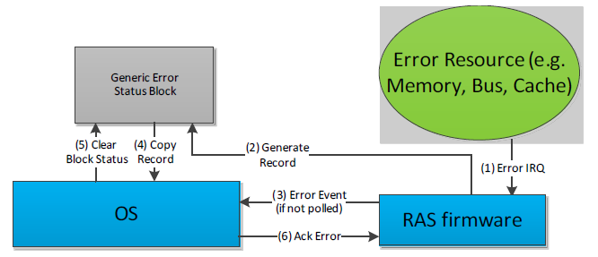
Fig. 18.1 APEI error flow example with external RAS controller
For GHESv2 error sources, the OSPM must acknowledge the consumption of the Error Status Block by writing to the “Read Ack Register” listed in the GHESv2 structure (described in the following table). For platforms that describe multiple Generic Hardware Error Sources, the platform must provide a unique memory region for the Error Status Block of each error source.
Name |
Byte Length |
Byte Offset |
Description |
|---|---|---|---|
Type |
2 |
0 |
10 - Generic Hardware Error Source (version 2) structure |
Equivalent fields in Table 18.10 |
62 |
2 |
Same format as fields in Table 18.10, starting from Source Id and ending in Error Status Block Length (inclusive). |
Read Ack Register |
12 |
64 |
Generic Address Structure as defined in Table 18.10. This field specifies the location of the Read Ack Register used to notify the RAS controller that OSPM has processed the Error Status Block. The OSPM writes the bit(s) specified in Read Ack Write, while preserving the bit(s) specified in Read Ack Preserve. |
Read Ack Preserve |
8 |
76 |
Contains a mask of bits to preserve when writing the Read Ack register. |
Read Ack Write |
8 |
84 |
Contains a mask of bits to set when writing the Read Ack register. |
These are the steps the OS must take once detecting an error from a particular GHESv2 error source:
OSPM detects error (via interrupt/exception or polling the block status)
OSPM copies the error status block
OSPM clears the block status field of the error status block
OSPM acknowledges the error via Read Ack register. For example:
OSPM reads the Read Ack register –> X
OSPM writes –> (( X & ReadAckPreserve) | ReadAckWrite)
18.3.2.9. Hardware Error Notification
This table describes the notification mechanism associated with a hardware error source.
Field |
Byte Length |
Byte Offset |
Description |
Type |
1 |
0 |
Identifies the notification type:
0 - Polled
1 - External Interrupt
2 - Local Interrupt
3 - SCI
4 - NMI
5 - CMCI
6 - MCE
7 - GPIO-Signal
8 - ARMv8 SEA
9 - ARMv8 SEI
10 - External Interrupt - GSIV
11 - Software Delegated Exception. For definitions of the fields in this structure for this type, see Links to ACPI-Related Documents (http://uefi.org/acpi) under the heading, “SDEI Specification.”
All other values are reserved
|
Length |
1 |
1 |
Total length of the structure in bytes. |
Configuration Write Enable |
2 |
2 |
This field indicates whether configuration parameters may be modified by OSPM. If the bit for the associated parameter is set, the parameter is writeable by OSPM:
Bit [0]: Type
Bit [1]: Poll Interval
Bit [2]: Switch To Polling Threshold Value
Bit [3]: Switch To Polling Threshold Window
Bit [4]: Error Threshold Value
Bit [5]: Error Threshold Window All other bits are reserved.
|
Poll Interval |
4 |
4 |
Indicates the poll interval in milliseconds OSPM should use to periodically check the error source for the presence of an error condition. |
Vector |
4 |
8 |
Interrupt vector. For type 10 “External Interrupt - GSIV”, this field specifies the GSIV triggered by the error source. For type 11 “Software Delegated Exception,” this field specifies the SDEI event number (see the SDEI Specification). |
Switch To Polling Threshold Value |
4 |
12 |
The number of error interrupts that must occur within Switch To Polling Threshold Interval before OSPM switches the error source to polled mode. |
Switch To Polling Threshold Window |
4 |
16 |
Indicates the time interval in milliseconds that Switch To Polling Threshold Value interrupts must occur within before OSPM switches the error source to polled mode. |
Error Threshold Value |
4 |
20 |
Indicates the number of error events that must occur within Error Threshold Interval before OSPM processes the event as an error condition. |
Error Threshold Window |
4 |
24 |
Indicates the time interval in milliseconds that Error Threshold Value errors must occur within before OSPM processes the event as an error condition. |
18.3.2.10. IA-32 Architecture Deferred Machine Check
Processors implementing the IA-32 Instruction Set Architecture may report Deferred errors to OSPM. These errors indicate that data has been corrupted but not consumed. The information in this table allows platform firmware to communicate key parameters of the deferred processor error reporting mechanism to OSPM, including whether Deferred Machine Check (DMC) processing should be enabled.
Only one entry of this type is permitted in the HEST. OSPM applies the information specified in this entry to all processors.
Field |
Byte Length |
Byte Offset |
Description |
|---|---|---|---|
Type |
2 |
0 |
11 - IA-32 Architecture Deferred Machine Check Structure. |
Source Id |
2 |
2 |
This value serves to uniquely identify this error source against other error sources reported by the platform. |
Reserved |
2 |
4 |
Reserved. |
Flags |
1 |
6 |
Bit [0] - FIRMWARE_FIRST: If set, this bit indicates to the OSPM that the interrupt handler from system firmware will run first for this error source.
Bit [2] - GHES_ASSIST: If set, this bit indicates that although OSPM is responsible for directly handling the error (as expected when FIRMWARE_FIRST is not set), system firmware may report additional information in the context of the error reported by hardware. The additional information is reported in a Generic Hardware Error Source structure with a matching Related Source ID. See Section 18.7, GHES_ASSIST Error Reporting. NOTE: If FIRMWARE_FIRST is set, this bit is reserved.
All other bits must be set to zero.
|
Enabled |
1 |
7 |
If the field value is 1, indicates this error source is to be enabled.
If the field value is 0, indicates that the error source is not to be enabled.
If FIRMWARE_FIRST is set in the flags field, the Enabled field is ignored by OSPM.
|
Number of Records To Pre-allocate |
4 |
8 |
Indicates the number of error records to pre-allocate for this error source. Must be >= 1. |
Max Sections Per Record |
4 |
12 |
Indicates the maximum number of error sections included in an error record created as a result of an error reported by this error source. Must be >= 1. |
Notification Structure |
28 |
16 |
Hardware Error Notification Structure, as defined in Table 18.14. |
Number Of Hardware Banks |
1 |
44 |
Indicates the number of hardware error reporting banks. |
Reserved |
3 |
45 |
Reserved. |
Machine Check Bank Structure[n] |
48 |
A list of Machine Check Bank structures defined in IA-32 Architecture Machine Check Bank Structure. |
18.3.2.11. Error Source Structure Header (Type 12 Onward)
Beginning with error source type 12 and onward, each Error Source Structure must use the standard Error Source Structure Header as defined below.
Field |
Byte Length |
Byte Offset |
Description |
Type |
2 |
0 |
Error Type |
Error Source Structure Length |
2 |
2 |
The length of the error source structure in bytes |
18.4. Firmware First Error Handling
It may be necessary for the platform to process certain classes of errors in firmware before relinquishing control to OSPM for further error handling. Errata management and error containment are two examples where firmware-first error handling is beneficial. Generic hardware error sources support this model through the related source ID.
The platform reports the original error source to OSPM via the hardware error source table (HEST) and sets the FIRMWAREFIRST flag for this error source. In addition, the platform must report a generic error source with a related source ID set to the original source ID. This generic error source is used to notify OSPM of the errors on the original source and their status after the firmware first handling.
There are different notification strategies that can be used in firmware first handling; the following options are available to the platform:
Traditional ACPI platforms may use NMI to notify the OSPM of both corrected and uncorrected errors for a given error source
Traditional ACPI platforms may use NMI to report uncorrected errors and the SCI to report corrected errors
Traditional ACPI platforms may use NMI to report uncorrected errors and polling to notify the OSPM of corrected errors
HW-reduced ACPI platforms may use GPIO-signaled events, Interrupt-signaled events, or polling to report corrected errors.
18.4.1. Example: Firmware First Handling Using NMI Notification
If the platform chooses to use NMI to report errors, which is the recommended method for uncorrected errors, the platform follows these steps:
System firmware configures the platform to trigger a firmware handler when the error occurs
System firmware identifies the error source for which it will handle errors via the error source enumeration interface by setting the FIRMWARE_FIRST flag
System firmware describes the generic error source, and the associated error status block, as described in Generic Hardware Error Source. System firmware identifies the relation between the generic error sourcde and the original error source by using the original source ID in the related source ID of Generic Hardware Error Source Structure.
When a hardware error reported by the error source occurs, system firmware gains control and handles the error condition as required. Upon completion system firmware should do the following:
Extract the error information from the error source and fill in the error information in the data block of the generic error source it identified as an alternate in step 3. The error information format follows the specification in Generic Error Data
Set the appropriate bit in the block status field (Generic Error Status Block ) to indicate to the OSPM that a valid error condition is present.
Clears error state from the hardware.
Generates an NMI.
At this point, the OSPM NMI handler scans the list of generic error sources to find the error source that reported the error and processes the error report
18.5. Error Serialization
The error record serialization feature is used to save and retrieve hardware error information to and from a persistent store. OSPM interacts with the platform through a platform interface. If the Error Record Serialization Table (ERST) is present, OSPM uses the ACPI solution described below. Otherwise, OSPM uses the UEFI runtime variable services to carry out error record persistence operations on UEFI based platforms.
For error persistence across boots, the platform must implement some form of non-volatile store to save error records. The amount of space required depends on the platform’s processor architecture. Typically, this store will be flash memory or some other form of non-volatile RAM.
Serialized errors are encoded according to the Common Platform Error Record (CPER) format, which is described in the appendices of the UEFI Specification. These entries are referred to as error records.
The Error Record Serialization Interface is designed to be sufficiently abstract to allow hardware vendors flexibility in how they implement their error record serialization hardware. The platform provides details necessary to communicate with its serialization hardware by populating the ERST with a set of Serialization Instruction Entries. One or more serialization instruction entries comprise a Serialization Action. OSPM carries out serialization operations by executing a series of Serialization Actions. Serialization Actions and Serialization Instructions are described in detail in the following sections.
The following table details the ERST layout, which system firmware is responsible for building.
Field |
Byte Length |
Byte Offset |
Description |
|---|---|---|---|
ACPI Standard Header |
|||
Header Signature |
4 |
0 |
“ERST”. Signature for the Error Record Serialization Table. |
Length |
4 |
4 |
Length, in bytes, of entire ERST. Entire table must be contiguous. |
Revision |
1 |
8 |
1 |
Checksum |
1 |
9 |
Entire table must sum to zero. |
OEMID |
6 |
10 |
OEM ID. |
OEM Table ID |
8 |
16 |
The manufacturer model ID. |
OEM Revision |
4 |
24 |
OEM revision of the ERST for the supplied OEM table ID. |
Creator ID |
4 |
28 |
Vendor ID of the utility that created the table. |
Creator Revision |
4 |
32 |
Revision of the utility that created the table. |
Serialization Header |
|||
Serialization Header Size |
4 |
36 |
Length in bytes of the serialization header. |
Reserved |
4 |
40 |
Must be zero. |
Instruction Entry Count |
4 |
44 |
The number of Serialization Instruction Entries in theSerialization Action Table. |
Serialization Action Table |
|||
Serialization Instruction Entries |
48 |
A series of error logging instruction entries. |
18.5.1. Serialization Action Table
A Serialization Action is defined as a series of Serialization Instructions on registers that result in a well known action. A Serialization Instruction is a Serialization Action primitive and consists of either reading or writing an abstracted hardware register. The Serialization Action Table contains Serialization Instruction Entries for all the Serialization Actions the platform supports.
In most cases, a Serialization Action comprises only one Serialization Instruction, but it is conceivable that a more complex device will require more than one Serialization Instruction. When an action does comprise more than one instruction, the instructions must be listed consecutively and they will consequently be performed sequentially, according to their placement in the Serialization Action Table.
18.5.1.1. Serialization Actions
This section identifies the Serialization Actions that comprise the Error Record Serialization interface, as shown in the following table.
Value |
Name |
Description |
|---|---|---|
0x0 |
BEGIN_WRITE_OPERATION |
Indicates to the platform that an error record write operation is beginning. This allows the platform to set its operational context. |
0x1 |
BEGIN_READ_OPERATION |
Indicates to the platform that an error record read operation is beginning. This allows the platform to set its operational context. |
0x2 |
BEGIN_CLEAR_OPERATION |
Indicates to the platform that an error record clear operation is beginning. This allows the platform to set its operation context. |
0x3 |
END_OPERATION |
Indicates to the platform that the current error record operation has ended. This allows the platform to clear its operational context. |
0x4 |
SET_RECORD_OFFSET |
Sets the offset from the base of the Error Log to transfer an error record. |
0x5 |
EXECUTE_OPERATION |
Instructs the platform to carry out the current operation based on the current operational context. |
0x6 |
CHECK_BUSY_STATUS |
Returns the state of the current operation. Once an operation has been executed through the EXECUTE_OPERATION action, the platform is required to return an indication that the operation is in progress until the operation completes. This allows the OS to poll for completion by repeatedly executing the CHECK_BUSY_STATUS action until the platform indicates that the operation not busy. |
0x7 |
GET_COMMAND_STATUS |
Returns the status of the current operation. The platform is expected to maintain a status code for each operation. Bits [8:1] of the value returned from the Register Region indicate the command status, which requires that the Bit Offset of the GAS for the Register Region is set to 1. See Command-Status-Definition for a list of valid command status codes. |
0x8 |
GET_RECORD_IDENTIFIER |
Returns the record identifier of an existing error record on the persistent store. The error record identifier is a 64-bit unsigned value as defined in the appendices of the UEFI Specification. If the record store is empty, this action must return 0xFFFFFFFFFFFFFFFF. |
0x9 |
SET_RECORD_IDENTIFIER |
Sets the record identifier. The error record identifier is a 64-bit unsigned value as defined in the appendices of the UEFI Specification. |
0xA |
GET_RECORD_COUNT |
Retrieves the number of error records currently stored on the platforms persistent store. The platform is expected to maintain a count of the number of error records resident in its persistent store. |
0xB |
BEGIN_DUMMY_WRITE-_OPERATION |
Indicates to the platform that a dummy error record write operation is beginning. This allows the platform to set its operational context. A dummy error record write operation performs no actual transfer of information from the Error Log Address Range to the persistent store. |
0xC |
RESERVED |
Reserved. |
0xD |
GET_ERROR_LOG-_ADDRESS_RANGE |
Returns the 64-bit physical address OSPM uses as the buffer for reading/writing error records. |
0xE |
GET_ERROR_LOG-_ADDRESS_RANGE_LENGTH |
Returns the length in bytes of the Error Log Address Range |
0xF |
GET_ERROR_LOG-_ADDRESS_RANGE_ATTRIBUTES |
Returns attributes that describe the behavior of the error log address range:
Bit [0] (0x1) - Reserved.
Bit [1] (0x2) - Non-Volatile: Indicates that the error log address range is in non-volatile RAM.
Bit [2] (0x4) - Slow: Indicates that the memory in which the error log address range is locates has slow access times.
All other bits reserved.
|
0x10 |
GET_EXECUTE-_OPERATION_TIMINGS |
Returns an encoded QWORD:
[63:32] value in microseconds that the platform expects would be the maximum amount of time it will take to process and complete an EXECUTE_OPERATION.
[31:0] value in microseconds that the platform expects would be the nominal amount of time it will take to process and complete an EXECUTE_OPERATION.
|
The following table defines the serialization action status codes returned from GET_COMMAND_STATUS.
Value |
Description |
|---|---|
0x00 |
Success |
0x01 |
Not Enough Space |
0x02 |
Hardware Not Available |
0x03 |
Failed |
0x04 |
Record Store Empty |
0x05 |
Record Not Found |
18.5.1.2. Serialization Instruction Entries
Each Serialization Action consists of a series of one or more Serialization Instructions. A Serialization Instruction represents a primitive operation on an abstracted hardware register represented by the register region as defined in a Serialization Instruction Entry.
A Serialization Instruction Entry describes a region in a serialization hardware register and the serialization instruction to be performed on that region. The following table details the layout of a Serialization Instruction Entry.
Field |
Byte Length |
Byte Offset |
Description |
|---|---|---|---|
Serialization Action |
1 |
N+0 |
The serialization action that this serialization instruction is a part of. |
Instruction |
1 |
N+1 |
Identifies the instruction to execute. See the Serialization Instructions table for a list of valid serialization instructions. |
Flags |
1 |
N+2 |
Flags that qualify the instruction. |
Reserved |
1 |
N+3 |
Must be zero. |
Register Region |
12 |
N+4 |
Generic Address Structure as defined in Section 5.2.3.2 to describe the address and bit. |
Value |
8 |
N+16 |
Value used with READ_REGISTER_VALUE and WRITE_REGISTER_VALUE instructions. |
Mask |
8 |
N+24 |
The bit mask required to obtain the bits corresponding to the serialization instruction in a given bit range defined by the register region. |
Register Region is described as a generic address structure. This structure describes the physical address of a register as well as the bit range that corresponds to a desired region of the register. The bit range is defined as the smallest set of consecutive bits that contains every bit in the register that is associated with the Serialization Instruction. If bits [6:5] and bits [3:2] all correspond to a Serialization Instruction, the bit range for that instruction would be [6:2].
Because a bit range could contain bits that do not pertain to a particular Serialization Instruction (i.e. bit 4 in the example above), a bit mask is required to distinguish all the bits in the region that correspond to the instruction. The Mask field is defined to be this bit mask with a bit set to ‘1’ for each bit in the bit range (defined by the register region) corresponding to the Serialization Instruction. Note that bit 0 of the bit mask corresponds to the lowest bit in the bit range. In the example used above, the mask would be 11011b or 0x1B.
The Instruction field identifies the operation to be performed on the register region by the instruction entry. The following table identifies the instructions that are supported.
Value |
Name |
Description |
|---|---|---|
0x00 |
READ_REGISTER |
A READ_REGISTER instruction reads the designated information from the specified Register Region. |
0x01 |
READ_REGISTER_VALUE |
A READ_REGISTER_VALUE instruction reads the designated information from the specified Register Region and compares the results with the contents of the Value field. If the information read matches the contents of the Value field, TRUE is returned, else FALSE is returned. |
0x02 |
WRITE_REGISTER |
A WRITE_REGISTER instruction writes a value to the specified Register Region. The Value field is ignored. |
0x03 |
WRITE_REGISTER_VALUE |
A WRITE_REGISTER_VALUE instruction writes the contents of the Value field to the specified Register Region. |
0x04 |
NOOP |
This instruction is a NOOP. |
0x05 |
LOAD_VAR1 |
Loads the VAR1 variable from the register region. |
0x06 |
LOAD_VAR2 |
Loads the VAR2 variable from the register region. |
0x07 |
STORE_VAR1 |
Stores the value in VAR1 to the indicate register region. |
0x08 |
ADD |
Adds VAR1 and VAR2 and stores the result in VAR1. |
0x09 |
SUBTRACT |
Subtracts VAR1 from VAR2 and stores the result in VAR1. |
0x0A |
ADD_VALUE |
Adds the contents of the specified register region to Value and stores the result in the register region. |
0x0B |
SUBTRACT_VALUE |
Subtracts Value from the contents of the specified register region and stores the result in the register region. |
0x0C |
STALL |
Stall for the number of microseconds specified in Value. |
0x0D |
STALL_WHILE_TRUE |
OSPM continually compares the contents of the specified register region to Value until the values are not equal. OSPM stalls between each successive comparison. The amount of time to stall is specified by VAR1 and is expressed in microseconds. |
0x0E |
SKIP_NEXT_INSTRUCTION_IF_TRUE |
This is a control instruction which compares the contents of the register region with Value. If the values match, OSPM skips the next instruction in the sequence for the current action. |
0x0F |
GOTO |
OSPM will go to the instruction specified by Value. The instruction is specified as the zero-based index. Each instruction for a given action has an index based on its relative position in the array of instructions for the action. |
0x10 |
SET_SRC_ADDRESS_BASE |
Sets the SRC_BASE variable used by the MOVE_DATA instruction to the contents of the register region. |
0x11 |
SET_DST_ADDRESS_BASE |
Sets the DST_BASE variable used by the MOVE_DATA instruction to the contents of the register region. |
0x12 |
MOVE_DATA |
Moves VAR2 bytes of data from SRC_BASE + Offset to DST_BASE + Offset, where Offset is the contents of the register region. |
The Flags field allows qualifying flags to be associated with the instruction. The following table identifies the flags that can be associated with Serialization Instructions.
Value |
Name |
Description |
|---|---|---|
0x01 |
PRESERVE_REGISTER |
For WRITE_REGISTER and WRITE_REGISTER_VALUE instructions, this flag indicates that bits within the register that are not being written must be preserved rather than destroyed. For READ_REGISTER instructions, this flag is ignored. |
18.5.1.2.1. READ_REGISTER_VALUE
A read register value instruction reads the register region and compares the result with the specified value. If the values are not equal, the instruction failed. This can be described in pseudo code as follows:
X = Read(register)
X = X >> Bit Offset described in Register Region
X = X & Mask
If (X != Value) FAIL
SUCCEED
18.5.1.2.2. READ_REGISTER
A read register instruction reads the register region. The result is a generic value and should not be compared with Value. Value will be ignored. This can be described in pseudo code as follows:
X = Read(register)
X = X >> Bit Offset described in Register Region
X = X & Mask
Return X
18.5.1.2.3. WRITE_REGISTER_VALUE
A write register value instruction writes the specified value to the register region. If PRESERVE_REGISTER is set in Instruction Flags, then the bits not corresponding to the write value instruction are preserved. If the register is preserved, the write value instruction requires a read of the register. This can be described in pseudo code as follows:
X = Value & Mask
X = X << Bit Offset described in Register Region
If (Preserve Register)
Y = Read(register)
Y = Y & ~(Mask << Bit Offset)
X = X \| Y
Write(X, Register)
18.5.1.2.4. WRITE_REGISTER
A write register instruction writes a value to the register region. Value will be ignored. If PRESERVE_REGISTER is set in Instruction Flags, then the bits not corresponding to the write instruction are preserved. If the register is preserved, the write value instruction requires a read of the register. This can be described in pseudo code as follows:
X = supplied value
X = X & Mask
X = X << Bit Offset described in Register Region
If (Preserve Register)
Y = Read(register)
Y = Y & ~(Mask << Bit Offset)
X = X \| Y
Write(X, Register)
18.5.1.3. Error Record Serialization Information
The APEI error record includes an 8 byte field called OSPM Reserved. The following table defines the layout of this field. The error record serialization information is a small buffer the platform can use for serialization bookkeeping. The platform is free to use the 48 bits starting at bit offset 16 for its own purposes. It may use these bits to indicate the busy/free status of an error record, to record an internal identifier, etc.
Field |
Bit Length |
Bit Offset |
Description |
|---|---|---|---|
Signature |
16 |
0 |
16-bit signature (‘ER’) identifying the start of the error record serialization data. |
Platform Serialization Data |
48 |
16 |
Platform private error record serialization information. |
18.5.2. Operations
The error record serialization interface comprises three operations: Write, Read, and Clear. OSPM uses the Write operation to write a single error record to the persistent store. The Read operation is used to retrieve a single error record previously recorded to the persistent store using the write operation. The Clear operation allows OSPM to notify the platform that a given error record has been fully processed and is no longer needed, allowing the platform to recover the storage associated with a cleared error record.
Where the Error Log Address Range is NVRAM, significant optimizations are possible since transfer from the Error Log Address Range to a separate storage device is unnecessary. The platform may still, however, copy the record from NVRAM to another device, should it choose to. This allows, for example, the platform to copy error records to private log files. In order to give the platform the opportunity to do this, OSPM must use the Write operation to persist error records even when the Error Log Address Range is NVRAM. The Read and Clear operations, however, are unnecessary in this case as OSPM is capable of reading and clearing error records without assistance from the platform.
18.5.2.1. Writing
To write a single HW error record, OSPM executes the following steps:
Initializes the error record’s serialization info. OSPM must fill in the Signature.
Writes the error record to be persisted into the Error Log Address Range.
Executes the BEGIN_WRITE_OPERATION action to notify the platform that a record write operation is beginning.
Executes the SET_RECORD_OFFSET action to inform the platform where in the
Error Log Address Range the error record resides.
Executes the EXECUTE_OPERATION action to instruct the platform to begin the write operation.
Busy waits by continually executing CHECK_BUSY_STATUS action until FALSE is returned.
Executes a GET_COMMAND_STATUS action to determine the status of the write operation. If an error is indicated, the OS
PM may retry the operation.
Executes an END_OPERATION action to notify the platform that the record write operation is complete.
When OSPM performs the EXECUTE_OPERATION action in the context of a record write operation, the platform attempts to transfer the error record from the designated offset in the Error Log Address Range to a persistent store of its choice. If the Error Log Address Range is non-volatile RAM, no transfer is required.
Where the platform is required to transfer the error record from the Error Log Address Range to a persistent store, it performs the following steps in response to receiving a write command:
Sets some internal state to indicate that it is busy. OSPM polls by executing a CHECK_BUSY_STATUS action until the operation is completed.
Reads the error record’s Record ID field to determine where on the storage medium the supplied error record is to be written. The platform attempts to locate the specified error record on the persistent store.
If the specified error record does not exist, the platform attempts to write a new record to the persistent store.
If the specified error record does exists, then if the existing error record is large enough to be overwritten by the supplied error record, the platform can do an in-place replacement. If the existing record is not large enough to be overwritten, the platform must attempt to locate space in which to write the new record. It may mark the existing record as Free and coalesce adjacent free records in order to create the necessary space.
Transfers the error record to the selected location on the persistent store.
Updates an internal Record Count if a new record was written.
Records the status of the operation so OSPM can retrieve the status by executing a GET_COMMAND_STATUS action.
Modifies internal busy state as necessary so when OS PM executes CHECK_BUSY_STATUS, the result indicates that the operation is complete.
If the Error Log Address Range resides in NVRAM, the minimum steps required of the platform are:
Sets some internal state to indication that it is busy. OSPM polls by executing a CHECK_BUSY_STATUS action until the operation is completed.
Records the status of the operation so OSPM can retrieve the status by executing a GET_COMMAND_STATUS action.
Clear internal busy state so when OS PM executes CHECK_BUSY_STATUS, the result indicates that the operation is complete.
18.5.2.2. Reading
During boot, OSPM attempts to retrieve all serialized error records from the persistent store. If the Error Log Address Range does not reside in NVRAM, the following steps are executed by OSPM to retrieve all error records:
Executes the BEGIN_ READ_OPERATION action to notify the platform that a record read operation is beginning.
Executes the SET_ RECORD_OFFSET action to inform the platform at what offset in the Error Log Address Range the error record is to be transferred.
Executes the SET_RECORD_IDENTIFER action to inform the platform which error record is to be read from its persistent store.
Executes the EXECUTE_OPERATION action to instruct the platform to begin the read operation.
Busy waits by continually executing CHECK_BUSY_STATUS action until FALSE is returned.
Executes a GET_COMMAND_STATUS action to determine the status of the read operation.
If the status is Record Store Empty (0x04), continue to step 7.
If an error occurred reading a valid error record, the status will be Failed (0x03), continue to step 7.
If the status is Record Not Found (0x05), indicating that the specified error record does not exist, OSPM retrieves a valid identifier by executing a GET_RECORD_IDENTIFIER action. The platform will return a valid record identifier.
If the status is Success, OSPM transfers the retrieved record from the Error Log Address Range to a private buffer and then executes the GET_RECORD_IDENTIFIER action to determine the identifier of the next record in the persistent store.
Execute an END_OPERATION to notify the platform that the record read operation is complete.
The steps performed by the platform to carry out a read request are as follows:
Sets some internal state to indicate that it is busy. OSPM polls by executing a CHECK_BUSY_STATUS action until the operation is completed.
Using the record identifier supplied by OSPM through the SET_RECORD_IDENTIFIER operation, determine which error record to read:
If the identifier is 0x0 (unspecified), the platform reads the ‘first’ error record from its persistent store (first being implementation specific).
If the identifier is non-zero, the platform attempts to locate the specified error record on the persistent store.
If the specified error record does not exist, set the status register’s Status to Record Not Found (0x05), and update the status register’s Identifier field with the identifier of the ‘first’ error record.
Transfer the record from the persistent store to the offset specified by OSPM from the base of the Error Log Address Range.
Record the Identifier of the ‘next’ valid error record that resides on the persistent store. This allows OSPM to retrieve a valid record identifier by executing a GET_RECORD_IDENTIFIER operation.
Record the status of the operation so OSPM can retrieve the status by executing a GET_COMMAND_STATUS action.
Clear internal busy state so when OSPM executes CHECK_BUSY_STATUS, the result indicates that the operation is complete.
Where the Error Log Address Range does reside in NVRAM, OSPM requires no platform support to read persisted error records. OSPM can scan the Error Log Address Range on its own and retrieve the error records it previously persisted.
18.5.2.3. Clearing
After OSPM has finished processing an error record, it will notify the platform by clearing the record. This allows the platform to delete the record from the persistent store or mark it such that the space is free and can be reused. The following steps are executed by OSPM to clear an error record:
Executes a BEGIN_ CLEAR_OPERATION action to notify the platform that a record clear operation is beginning.
Executes a SET_RECORD_IDENTIFER action to inform the platform which error record is to be cleared. This value must not be set to 0x0 (unspecified).
Executes an EXECUTE_OPERATION action to instruct the platform to begin the clear operation.
Busy waits by continually executing CHECK_BUSY_STATUS action until FALSE is returned.
Executes a GET_COMMAND_STATUS action to determine the status of the clear operation.
Execute an END_OPERATION to notify the platform that the record read operation is complete.
The platform carries out a clear request by performing the following steps:
Sets some internal state to indication that it is busy. OSPM polls by executing a CHECK_BUSY_STATUS action until the operation is completed.
Using the record identifier supplied by OSPM through the SET_RECORD_IDENTIFIER operation, determine which error record to clear. This value may not be 0x0 (unspecified).
Locate the specified error record on the persistent store.
Mark the record as free by updating the Attributes in its serialization header.
Update internal record count.
Clear internal busy state so when OS PM executes CHECK_BUSY_STATUS, the result indicates that the operation is complete.
When the Error Log Address Range resides in NVRAM, the OS requires no platform support to Clear error records.
18.5.2.4. Usage
This section describes several possible ways the error record serialization mechanism might be implemented.
18.5.2.4.1. Error Log Address Range Resides in NVRAM
If the Error Log Address Range resides in NVRAM, then when OSPM writes a record into the logging range, the record is automatically persistent and the busy bit can be cleared immediately. On a subsequent boot, OSPM can read any persisted error records directly from the persistent store range. The size of the persistent store, in this case, is expected to be enough for several error records.
18.5.2.4.2. Error Log Address Range Resides in (volatile) RAM
In this implementation, the Error Log Address Range describes an intermediate location for error records. To persist a record, OSPM copies the record into the Error Log Address Range and sets the Execute, at which time the platform runs necessary code (SMM code on non-UEFI based systems and UEFI runtime code on UEFI-enabled systems) to transfer the error record from main memory to some persistent store. To read a record, OSPM asks the platform to copy a record from the persistent store to a specified offset within the Error Log Address Range. The size of the Error Log Address Range is at least large enough for one error record.
18.5.2.4.3. Error Log Address Range Resides on Service Processor
In this type of implementation, the Error Log Address Range is really MMIO. When OSPM writes an error record to the Error Log Address Range, it is really writing to memory on a service processor. When the OSPM sets the Execute control bit, the platform knows that the OSPM is done writing the record and can do something with it, like move it into a permanent location (i.e. hard disk) on the service processor. The size of the persistent store in this type of implementation is typically large enough for one error record.
18.5.2.4.4. Error Log Address Range is Copied Across Network
In this type of implementation, the Error Log Address Range is an intermediate cache for error records. To persist an error record, OSPM copies the record into the Error Log Address Range and set the Execute control bit, and the platform runs code to transmit this error record over the wire. The size of the Error Log Address Range in this type of implementation is typically large enough for one error record.
18.6. Error Injection
This section outlines an ACPI table mechanism, called EINJ, which allows for a generic interface mechanism through which OSPM can inject hardware errors to the platform without requiring platform specific OSPM level software. The primary goal of this mechanism is to support testing of OSPM error handling stack by enabling the injection of hardware errors. Through this capability OSPM is able to implement a simple interface for diagnostic and validation of errors handling on the system.
18.6.1. Error Injection Table (EINJ)
The Error Injection (EINJ) table provides a generic interface mechanism through which OSPM can inject hardware errors to the platform without requiring platform specific OSPM software. System firmware is responsible for building this table, which is made up of Injection Instruction entries. The following table describes the necessary details for EINJ.
Field |
Byte length |
Byte offset |
Description |
|---|---|---|---|
ACPI Standard Header |
|||
Header Signature |
4 |
0 |
EINJ. Signature for the Error Record Injection Table. |
Length |
4 |
4 |
Length, in bytes, of entire EINJ. Entire table must be contiguous. |
Revision |
1 |
8 |
2 |
Checksum |
1 |
9 |
Entire table must sum to zero. |
OEMID |
6 |
10 |
OEM ID. |
OEM Table ID |
8 |
16 |
The manufacturer model ID. |
OEM Revision |
4 |
24 |
OEM revision of EINJ. |
Creator ID |
4 |
28 |
Vendor ID of the utility that created the table. |
Creator Revision |
4 |
32 |
Revision of the utility that created the table. |
Injection Header |
|||
Injection Header Size |
4 |
36 |
Length in bytes of the Injection Interface header. |
Injection Flags |
1 |
40 |
Reserved. Must be zero |
Reserved |
3 |
41 |
Must be zero. |
Injection Entry Count |
4 |
44 |
The number of Instruction Entries in the Injection Action Table |
Injection Action Table |
|||
Injection Instruction Entries |
48 |
A series of error injection instruction entries, per Injection Entry Count See Table 18.26. |
The following table identifies the supported error injection actions.
Value |
Name |
Description |
0x0 |
BEGIN_INJECTION_OPERATION |
Indicates to the platform that an error injection is beginning. This allows the platform to set its operational context.
|
0x1 |
GET_TRIGGER_ERROR_ACTION-_TABLE |
Returns a 64-bit physical memory pointer to the Trigger Action Table. See Table 18.36
|
0x2 |
SET_ERROR_TYPE |
Type of error to Inject. Only one ERROR_TYPE can be injected at any given time. If there is request for multiple injections at the same time, then the platform will return an error condition. See Section 18.6.4.
|
0x3 |
GET_ERROR_TYPE |
Returns the error injection capabilities of the platform.
|
0x4 |
END_OPERATION |
Indicates to the platform that the current injection operation has ended. This allows the platform to clear its operational context.
|
0x5 |
EXECUTE_OPERATION |
Instructs the platform to carry out the current operation based on the current operational context.
|
0x6 |
CHECK_BUSY_STATUS |
Returns the state of the current operation. Once an operation has been executed through the EXECUTE_OPERATION action, the platform is required to return an indication that the operation is busy until the operation is completed. This allows software to poll for completion by repeatedly executing the CHECK_BUSY_STATUS action until the platform indicates that the operation is complete by setting not busy.
The lower most bit (bit0) of the returned value indicates the busy status by setting it to 1 and not busy status by setting it to 0.
|
0x7 |
GET_COMMAND_STATUS |
Returns the status of the current operation. See Table 18.29 for a list of valid command status codes. |
0x8 |
SET_ERROR_TYPE-_WITH_ADDRESS |
Type of error to Inject, and the address to inject. Only one Error type can be injected at any given time. If there is request for multiple injections at the same time, then the platform will return an error condition.
The RegisterRegion field (See Table 18.26) in SET_ERROR_TYPE_WITH_ADDRESS points to a data structure whose format is defined in Table 18.31.
Note that executing SET_ERROR_TYPE_WITH_ADDRESS without specifying an address has the same effect as executing SET_ERROR_TYPE. See Table 18.30, error type definition.
|
0x9 |
GET_EXECUTE_OPERATION-_TIMINGS |
Returns an encoded QWORD: [63:32] value in microseconds that the platform expects would be the maximum amount of time it will take to process and complete an EXECUTE_OPERATION. [31:0] value in microseconds that the platform expects would be the nominal amount of time it will take to process and complete an EXECUTE_OPERATION.
|
0x10 |
EINJV2_SET_ERROR_TYPE |
New Error Injection action introduced in EINJv2 for the purpose of injecting an EINJv2 error type, with address, severity, and detailed syndrome. Only one Error type can be injected at any given time. For multiple injections at the same time, then the platform will return an error condition.
The RegisterRegion field (see Table 18.26) in EINJV2_SET_ERROR_TYPE points to a data structure whose format is defined in Table 18.34
See Section 18.6.4.1, for the EINJv2 error type definition.
|
0x11 |
EINJV2_GET_ERROR_TYPE |
Returns the extended error injection capabilities (EINJv2 features) of the platform:
Bit 0 - EINJv2 Processor Error Type supported
Bit 1 - EINJv2 Memory Error Type supported
Bit 2 - EINJv2 PCIe Error Type supported
Bit 3-30 - Reserved (Must be zero)
Bit 31 - EINJv2 Vendor specific error codes
|
0xFF |
TRIGGER_ERROR |
This Value is reserved for entries declared in the Trigger Error Action Table returned in response to a GET_TRIGGER_ERROR_ACTION_TABLE action. The returned table consists of a series of actions each of which is set to TRIGGER_ERROR (see Table 18.36). When executed by software, the series of TRIGGER_ERROR actions triggers the error injected as a result of the successful completion of an EXECUTE_OPERATION action.
|
18.6.2. Injection Instruction Entries
An Injection action consists of a series of one or more Injection Instructions. An Injection Instruction represents a primitive operation on an abstracted hardware register, represented by the register region as defined in an Injection Instruction Entry.
An Injection Instruction Entry describes a region in an injection hardware register and the injection instruction to be performed on that region.
The following table details the layout of an Injection Instruction Entry.
Field |
Byte length |
Byte offset |
Description |
|---|---|---|---|
Injection Action |
1 |
0 |
The injection action that this instruction is a part of. See the Error Injection Actions table for supported injection actions. |
Instruction |
1 |
1 |
Identifies the instruction to execute. See the Injection Instructions table for a list of valid instructions. |
Flags |
1 |
2 |
Flags that qualify the instruction. |
Reserved |
1 |
3 |
Must be zero. |
Register Region |
12 |
4 |
The Generic Address Structure is used to describe the address and bit. Address_Space_ID must be 0 (System Memory) or 1 (System IO). This constraint is an attempt to ensure that the registers are accessible in the presence of hardware error conditions. |
Value |
8 |
16 |
This is the value field that is used by the instruction READ or WRITE_REGISTER_VALUE. |
Mask |
8 |
24 |
The bit mask required to obtain the bits corresponding to the injection instruction in a given bit range defined by the register region. |
Register Region is described as a generic address structure. This structure describes the physical address of a register as well as the bit range that corresponds to a desired region of the register. The bit range is defined as the smallest set of consecutive bits that contains every bit in the register that is associated with the injection Instruction. If bits [6:5] and bits [3:2] all correspond to an Injection Instruction, the bit range for that instruction would be [6:2].
Because a bit range could contain bits that do not pertain to a particular injection Instruction (i.e. bit 4 in the example above), a bit mask is required to distinguish all the bits in the region that correspond to the instruction. The Mask field is defined to be this bit mask with a bit set to a ‘1’ for each bit in the bit range (defined by the register region) corresponding to the Injection Instruction. Note that bit 0 of the bit mask corresponds to the lowest bit in the bit range. In the example used above, the mask would be 11011b or 0x1B.
Value |
Name |
Description |
|---|---|---|
0x01 |
PRESERVE_REGISTER |
For WRITE_REGISTER and WRITE_REGISTER_VALUE instructions, this flag indicates that bits within the register that are not being written must be preserved rather than destroyed. For READ_REGISTER instructions, this flag is ignored. |
18.6.3. Injection Instructions
The table below lists the supported Injection Instructions for Injection Instruction Entries.
Opcode |
Instruction name |
Description |
|---|---|---|
0x00 |
READ_REGISTER |
A READ_REGISTER instruction reads the value from the specified register region. |
0x01 |
READ_REGISTER_VALUE |
A READ_REGISTER_VALUE instruction reads the designated information from the specified Register Region and compares the results with the contents of the Value field. If the information read matches the contents of the Value field, TRUE is returned, else FALSE is returned. |
0x02 |
WRITE_REGISTER |
A WRITE_REGISTER instruction writes a value chosen by software to the specified Register Region. The Value field is ignored. |
0x03 |
WRITE_REGISTER_VALUE |
A WRITE_REGISTER_VALUE instruction writes the contents of the Value field to the specified Register Region. |
0x04 |
NOOP |
No operation. |
The table below defines the error injection status codes returned from GET_COMMAND_STATUS.
Value |
Description |
|---|---|
0x0 |
Success |
0x1 |
Unknown Failure |
0x2 |
Invalid Access |
18.6.4. Error Types
The table below defines the error type codes returned from GET_ERROR_TYPE, as well as the error type set by SET_ERROR_TYPE and the Error Type field set by SET_ERROR_TYPE_WITH_ADDRESS (see Table 18.31).
Both the SET_ERROR_TYPE and SET_ERROR_TYPE_WITH_ADDRESS actions must be present as part of the EINJ Action Table. OSPM is free to choose either of these two actions to inject an error type. The platform will give precedence to SET_ERROR_TYPE_WITH_ADDRESS. That is, if a non-zero Error Type value is set by SET_ERROR_TYPE_WITH_ADDRESS, then any Error Type value set by SET_ERROR_TYPE will be ignored. But if no Error Type is specified by SET_ERROR_TYPE_WITH_ADDRESS, then the platform will use SET_ERROR_TYPE to identify the error type to inject.
Bit |
Description |
0 |
Processor Correctable |
1 |
Processor Uncorrectable non-fatal |
2 |
Processor Uncorrectable fatal |
3 |
Memory Correctable |
4 |
Memory Uncorrectable non-fatal |
5 |
Memory Uncorrectable fatal |
6 |
PCI Express Correctable |
7 |
PCI Express Uncorrectable non-fatal |
8 |
PCI Express Uncorrectable fatal |
9 |
Platform Correctable |
10 |
Platform Uncorrectable non-fatal |
11 |
Platform Uncorrectable fatal |
12 |
CXL.cache Protocol Correctable |
13 |
CXL.cache Protocol Uncorrectable non-fatal |
14 |
CXL.cache Protocol Uncorrectable fatal |
15 |
CXL.mem Protocol Correctable |
16 |
CXL.mem Protocol Uncorrectable non-fatal |
17 |
CXL.mem Protocol Uncorrectable fatal |
18:29 |
RESERVED |
30 |
EINJv2 Error Type. If this bit is set, then the support for EINJV2_SET_ERROR_TYPE and EINJV2_GET_ERROR_TYPE actions are supported.
NOTE: This may only be used with the action GET_ERROR_TYPE and it is not permitted to set this bit with SET_ERROR_TYPE or SET_ERROR_TYPE_WITH_ADDRESS
|
31 |
Vendor Defined Error Type. If this bit is set, then the Error types and related data structures are defined by the Vendor, as shown in Table 18.32. |
Note
CXL errors (Bits 17:12) are intended to target the CXL port (for example via Link or Protocol errors, not actual Component errors).
Field |
Byte Length |
Byte Offset |
Description |
Error Type |
4 |
0 |
Bitmap of error types to inject. See Table 18.30. This field is cleared by the platform once it is consumed. |
Vendor Error Type Extension Structure Offset |
4 |
4 |
Specifies the offset from the beginning of the table to the vendor error type extension structure. If no vendor error type extension is present, bit31 in error type must be clear and this field must be set to 0. |
Flags |
4 |
8 |
Bit [0] - Processor Identification Field Valid
Bit [1]- Memory Address and Memory address Mask Field Valid
NOTE: For CXL errors, the Memory Address points to a CXL 1.1 compliant memory-mapped Downstream port
Bit [2] - PCIe SBDF field valid
NOTE: For CXL errors, the SBDF points to a CXL 2.0 compliant Root port.
Bit [31:3] - RESERVED
This field is cleared by the platform once it is consumed.
|
Processor Error |
|||
Processor Identification |
4 |
12 |
Optional field: on non-ARM architectures, this is the physical APIC ID or the X2APIC ID of the processor which is a target for the injection; on ARM systems, this is the ACPI Processor UID value as used in the MADT. |
Memory Error |
|||
Memory Address |
8 |
16 |
Optional field specifying the physical address of the memory that is the target for the injection. Valid if Bit [1] of the Flags field is set. |
Memory Address Range |
8 |
24 |
Optional field that provides a range mask for the address field. Valid if Bit [1] of the Flags field is set. If the OSPM doesn’t want to provide a range of addresses, then this field should be zero. |
PCIe SBDF |
4 |
32 |
Byte 3 - PCIe Segment
Byte 2 - Bus Number
Byte 1:
Bits [7:3] Device Number
Bits [2:0] Function Number
Byte 0 - RESERVED
|
Field |
Byte Length |
Byte Offset |
Attribute |
Description |
|---|---|---|---|---|
Length |
4 |
0x0 |
Set by Platform. RO for Software. |
Length, in bytes, of the entire Vendor Error Type Extension Structure. |
SBDF |
4 |
0x04 |
Set by Platform. RO for Software |
This provides a PCIe Segment, Bus, Device and Function number which can be used to read the Vendor ID, Device ID and Rev ID, so that software can identify the system for error injection purposes. The platform sets this field and is RO for Software. |
Vendor ID |
2 |
0x08 |
Set by Platform. RO for Software |
Vendor ID which identifies the device manufacturer. This is the same as the PCI SIG defined Vendor ID. The platform sets this field and is RO for Software |
Device ID |
2 |
0x0A |
Set by Platform. RO for Software |
This 16-bit ID is assigned by the manufacturer that identifies this device. The platform sets this field and is RO for Software |
Rev ID |
1 |
0x0C |
Set by Platform. RO for Software |
This 8-bit value is assigned by the manufacturer and identifies the revision number of the device. The platform sets this field and is RO for Software |
Reserved |
3 |
0x0D |
Set by Platform. RO for Software |
Reserved |
OEM Defined structure |
N |
0x10 |
The rest of the fields are defined by the OEM. |
18.6.4.1. EINJv2 Error Types
EINJ version 2 (EINJv2) introduces a new error injection action The table below defines the error type codes returned from EINJV2_GET_ERROR_TYPE, as well as the error type set by EINJV2_SET_ERROR_TYPE.
EINJV2_SET_ERROR_TYPE actions must be present as part of the EINJ Action Table. OSPM is free to choose this action for advanced error injection options. The platform will give precedence to EINJV2_SET_ERROR_TYPE. That is, if a non-zero Error Type value is set by EINJV2_SET_ERROR_TYPE, then any Error Type value set by SET_ERROR_TYPE_WITH_ADDRESS and/or SET_ERROR_TYPE will be ignored.
Also, EINJv2 breaks out the Error Type from the severity. The following table describes the new Error Type encoding.
Bit |
Description |
0 |
Processor Error |
1 |
Memory Error |
2 |
PCIe Error |
3-30 |
Reserved |
31 |
Vendor Defined Error |
Field |
Byte Length |
Byte Offset |
Description |
Error Type |
4 |
0 |
Bit map of error types to inject (see Table 18.30). Only one Error Type bit may be set at a time. This field is cleared by the platform once it is consumed. |
Error Type Code |
1 |
4 |
Vendor specific code for each error type used to indicate error injection behavior. Value of zero is default error injection behavior as defined by EINJv2. Non-zero value indicates vendor specific behavior. |
Flags |
3 |
5 |
This field indicates which of the remaining fields are valid:
Bit 0 - Address Valid
Bit 1 - Address Range Valid
Bit 2 - Severity Valid
Bit 3 - Component Syndrome Count and Array is valid
All other bits are reserved
|
Length |
4 |
8 |
This specifies the length of the entire structure including the component syndrome array. |
Severity |
4 |
12 |
Optional field specifying the severity of the injected error:
0 - Corrected Error
1 - Uncorrected Non-Fatal
2 - Uncorrected Fatal
All other values are reserved
|
Address |
8 |
16 |
Optional field specifying the physical address of the memory that is the target for the injection. Valid if Bit [0] of the Flags field is set. |
Address Range |
8 |
24 |
Optional field specifying the physical address range mask of the memory that is the target for the injection. Valid if Bit [1] of the Flags field is set. |
Component Syndrome Count (N) |
4 |
28 |
This represents the maximum number of components supported in the Component Syndrome Array. This is intended to support injecting an error into multiple components / devices simultaneously. For Example: If Component Syndrome Count is valid per the Flags field and the value Count (N) is 4, this structure contains the error Component Syndrome Array for 4 unique components. |
Component Syndrome Array |
N * 32 |
32 |
This is an array based on the Component Syndrome Entry Structure, each entry being 32-bytes as described in Table 18.35. The length of this structure is 32 x Component Syndrome Count. |
Field |
Byte Length |
Byte Offset |
Description |
Component ID |
16 |
0 |
Component ID definition depends on the Error Type Value. Note that because this is a union structure, the byte length is 16 bytes to accommodate the largest possible ID (i.e. FRU ID for vendor specific errors).
Processor Error (0x1):
The bottom 32-bit represents the ACPI ID (represented in MADT) of the processor.
The remaining bits are vendor specific.
Memory Error (0x2):
This represents the Device ID within the memory module (e.g. DDR DIMM) for a particular system physical address. For example: 18 x 4 DIMMs support up to 18 devices (0-17) per address. 9 x 8 DIMMs support up to 9 devices (0-8) per address.
It is possible to inject error syndrome into multiple device instances up to the Component Syndrome Count.
PCIe Error (0x4):
This represents the SBDF.
Vendor Specific Error (0x80000000)
This represents some platform specific identifier (e.g. FRU ID or other vendor specific error format).
|
Component Syndrome |
16 |
16 |
The Component Syndrome definition depends on the Error Type Value.
Processor Error (0x1):
The usage of the syndrome bits will be vendor specific.
Memory Error (0x2):
This indicates bit mask of data bits that must be flipped within a memory device. (e.g. If the set syndrome bit value is zero, the bit value will be changed to one. if the set syndrome bit value is one, the bit value will be changed to zero). The range of valid bits depends on the component error injection granularity.
Example 1: For a DDR4 18x4 memory device topology with a burst length of 8 (e.g., 64-byte cache line in a single burst), there will be up to 32 valid bits per device that may be modified per burst. If bit 3 in this mask is set, bit offset 3 of the device in that burst will be flipped.
Example 2: For a DDR5 5x8 memory device topology with a burst length of 16 (e.g., 64-byte cache line in a single burst), there will be up to 128 valid bits per device that may be modified per burst.
PCIe Error (0x4):
The usage of the syndrome bits will be vendor specific.
Vendor Specific Error (0x80000000)
The usage of the syndrome bits will be vendor specific.
|
18.6.5. Trigger Action Table
An error injection operation is a two-step process where the error is injected into the platform and subsequently triggered. After software injects an error into the platform using the EXECUTE_OPERATION action, it then needs to trigger the error. In order to trigger the error, software executes the GET_TRIGGER_ERROR_ACTION_TABLE action, which returns a pointer to a Trigger Error Action table. The format of this table is shown in the table below. Software then executes the instruction entries specified in the Trigger Error Action Table in order to trigger the injected error.
TRIGGER_ERROR Header |
Byte Length |
Byte Offset |
Description |
|---|---|---|---|
Header Size |
4 |
0 |
Length in bytes of this header. |
Revision |
4 |
4 |
|
Table Size |
4 |
8 |
Size in Bytes of the entire table. |
Entry Count |
4 |
12 |
The number of Instruction Entries in the TRIGGER_ERROR Action Sequence - see note (1) below. |
Action Table |
|||
TRIGGER_ERROR Instruction Entries - see note (2) below |
16 |
A series of error injection instruction entries as defined in Table 18-405. |
Note
(1) If the “Entry Count” field above is ZERO, then there are no action structures in the TRIGGER_ERROR action table. The platform may make this field ZERO in situations where there is no need for a TRIGGER_ERROR action (for example, in cases where the error injection action seeds as well as consumes the error).
Note
(2) The format of TRIGGER_ERROR Instructions Entries is the same as Injection Instruction entries as described in Table 18-407.
18.6.6. Error Injection Operation
Before OSPM can use this mechanism to inject errors, it must discover the error injection capabilities of the platform by executing a GET_ERROR_TYPE. See Table 18.30 for a definition of error types.
After discovering the error injection capabilities, OSPM can inject and trigger an error according to the sequence described below.
Note that injecting an error into the platform does not automatically consume the error. In response to an error injection, the platform returns a trigger error action table. The software that injected the error must execute the actions in the trigger error action table in order to consume the error. If a specific error type is such that it is automatically consumed on injection, the platform will return a trigger error action table consisting of NO_OP.
Executes a BEGIN_INJECTION_OPERATION action to notify the platform that an error injection operation is beginning.
Executes a GET_ERROR_TYPE action to determine the error injection capabilities of the system. This action returns a DWORD bit map of the error types supported by the platform (see Table 18.30).
If GET_ERROR_TYPE returns the DWORD with Bit [31] set, it means that vendor defined error types are present, apart from the standard error types (see Table 18.30).
OSPM chooses the type of error to inject by executing a SET_ERROR_TYPE or a SET_ERROR_TYPE_WITH_ADDRESS _WITH_ADDRESS action (see Section 18.6.4).
If the OSPM chooses to inject one of the supported standard error types, then it sets the corresponding bit in the error type bitmap. For example, if OSPM chooses to inject a “Memory Correctable” error, then the OSPM sets the value 0x0000_0080 in the error type bitmap.
If the OSPM chooses to inject one of the vendor defined error types, then it sets bit[31] in the error type bitmap.
* OSPM exectures the SET_ERROR_TYPE_WITH_ADDRESS_WITH_ADDRESS action to retrieve the location of the “SET_ERROR_TYPE_WITH_ADDRESS data structure”, to then get the location of the “Vendor Error Type Extension Structure” by reading the “Vendor Error Type Extension Structure Offset” (see Table 18.32).
- OSPM reads the Vendor ID, Device ID and Rev ID from the PCI config space whose path (PCIe Segment/Device/Function) is provided in the “SBDF” field of the Vendor Error Type Extension Structure.
- If the Vendor ID/Device ID and Rev IDs match, then the OSPM can identify the platform it is running on and would know the Vendor error types that are supported by this platform.
- The OSPM writes the vendor error type to inject in the “OEM Defined Structure” field (see Table 18.32).
* Optionally, for either standard or vendor-defined error types, the OSPM can choose the target of the injection, such as a memory range, PCIe Segment/Device/Function or Processor APIC ID, depending on the type of error. The OSPM does this by executing the SET_ERROR_TYPE_WITH_ADDRESS action to fill in the appropriate fields of the “SET_ERROR_TYPE_WITH_ADDRESS Data structure” (see Table 18.31).
Executes an EXECUTE_OPERATION action to instruct the platform to begin the injection operation.
Busy waits by continually executing CHECK_BUSY_STATUS action until the platform indicates that the operation is complete by clearing the abstracted Busy bit.
Executes a GET_COMMAND_STATUS action to determine the status of the completed operation.
If the status indicates that the platform cannot inject errors, stop.
Executes a GET_TRIGGER_ERROR_ACTION_TABLE operation to get the physical pointer to the TRIGGER_ERROR action table. This provides the flexibility in systems where injecting an error is a two (or more) step process.
Executes the actions specified in the TRIGGER_ERROR action table.
Execute an END_OPERATION to notify the platform that the error injection operation is complete.
18.6.7. Error Injection Version 2 Operation
Before OSPM can use this mechanism to inject errors, it must discover the error injection capabilities of the platform by executing a EINJV2_GET_ERROR_TYPE. See Table 18.30 for a definition of error types.
After discovering the EINJv2 error injection capabilities, OSPM can inject and trigger an error according to the sequence described below.
Note that injecting an error into the platform does not automatically consume the error. In response to an error injection, the platform returns a trigger error action table. The software that injected the error must execute the actions in the trigger error action table in order to consume the error. If a specific error type is such that it is automatically consumed on injection, the platform will return a trigger error action table consisting of NO_OP:
Executes a BEGIN_INJECTION_OPERATION action to notify the platform that an error injection operation is beginning.
Executes a EINJ_GET_ERROR_TYPE action to determine the error injection capabilities of the system. This action returns a DWORD bit map of the error types supported by the platform (see Table 18.30).
If EINJV2_GET_ERROR_TYPE returns the DWORD with Bit [30] set, it means that EINJv2 error types are present, apart from the standard error types (see Table 18.30).
Executes a EINJV2_GET_ERROR_TYPE action to determine the error injection capabilities of the system. This action returns a DWORD bit map of the error types supported by the platform (see Table 18.33).
If EINJV2_GET_ERROR_TYPE returns the DWORD with Bit [1] set, it means that memory error types are present.
OSPM chooses the type of error to inject by executing a EINJV2_SET_ERROR_TYPE action.
If the OSPM chooses to inject one of the supported standard error types, then it sets the corresponding bit in the error type bitmap.
For example: if OSPM chooses to inject a Memory error, then the OSPM sets the value 0x0000_0002 in the error type bitmap. If OSPM chooses to inject a memory error pattern into a device at a particular DRAM address, the Flags will be set to 0x9 to indicate component syndrome and address are valid. OSPM will populate the Address field with the system physical address and the component syndrome count and array syndrome.
Error Type = 0x2 (Memory Error)
Error Code = 0x0 (no vendor specific behavior)
Length=0x44
Severity=0 (not used)
Address=0000FFFFFFF00000
Address Range=0x0
Flags = 0x9 (Address and Component Syndrome Array is Valid)
Component Syndrome Count = 1
Component Syndrome Array [0] = { 00000000000000000000000000000004 , 000000000000000000000000A5A5A5A5 }
So in this example software is trying to inject a 32-bit bit flip pattern on one device across a single burst for a particular system physical address. EINJV2_SET_ERROR_TYPE=000000000000000000000000A5A5A5A5000000000000000000000000000000040000000100000000000000000000FFFFFFF000000000000000000044000009000000002
Executes an EXECUTE_OPERATION action to instruct the platform to begin the injection operation.
Busy waits by continually executing CHECK_BUSY_STATUS action until the platform indicates that the operation is complete by clearing the abstracted Busy bit.
Executes a GET_COMMAND_STATUS action to determine the status of the completed operation.
If the status indicates that the platform cannot inject errors, stop.
18.7. GHES_ASSIST Error Reporting
In some cases, errors reported by hardware may provide a limited amount of information, as additional information may require platform-specific knowledge. Hence, the GHES_ASSIST mechanism, as marked in the Flags field of a given Error Source Structure, allows system firmware to provide additional information in the context of an error reported by hardware. Specifically, system firmware provides additional information via a Generic Hardware Error Source (GHES) structure which has its Related Source ID pointing back to the Error Source structure that represents the hardware. OSPM conveys support for GHES_ASSIST as declared by the GHES_ASSIST Support flag of the Platform-Wide _OSC Capabilities DWORD 2. See Section 6.2.11.2, Platform-Wide OSPM Capabilities.
Note
System firmware must ensure that additional information provided by GHES_ASSIST structures is aligned with the current error status information reported by the hardware. The implication is that as errors are generated by the hardware, system firmware must have mechanisms to get control before those errors are delivered to OSPM.
Since OSPM is expected to consume the additional GHES_ASSIST information in the context of an error reported by hardware, the Notification Structure associated with the pertinent GHES should have the Type field set to Polled, or a to type that is aligned with the signaling of the hardware error event. See Table 18.14, Hardware Error Notification Structure.
OSPM is expected clear the hardware error condition after consuming any additional information from the pertinent GHES_ASSIST structures.
18.7.1. GHES_ASSIST on Machine Check Architecture
To support GHES_ASSIST on Machine Check Architecture (MCA) error sources, system firmware provides a set of GHES structures for each MCA error source (see Table 18.3 Machine Check Exception, Table 18.5 Corrected Machine Check, and Table 18.15 Deferred Machine Check). Each set consists of a GHES structure per MCA bank on each Logical Processor (CPU), where the GHES structures from each set share a common Related Source ID.
For each MCA error source, OSPM can index thorough the set of GHES_ASSIST structures using the following formula:
Index = ((CPU number) * (MCA Banks per CPU)) + (MCA Bank index)
Where CPU number represents the index of the corresponding Processor Local APIC or x2APIC structure with (Flags.Enabled = 1) in MADT (e.g. 0 represents the first enabled Processor Local APIC or x2APIC entry in MADT), and MCA Banks per CPU represents the value of the Number Of Hardware Banks field from the pertinent MCA error source structure.
Note
System firmware must ensure that each set of GHES_ASSIST structures is laid out sequentially in system memory, so that OSPM may consume them as specified by the Index formula described above.