8.1. Processor Power States
ACPI defines the power state of system processors while in the G0 working state as being either active executing or sleeping (not executing) - see note below. Processor power states include are designated C0, C1, C2, C3, …Cn. The C0 power state is an active power state where the CPU executes instructions. The C1 through Cn power states are processor sleeping states where the processor consumes less power and dissipates less heat than leaving the processor in the C0 state. While in a sleeping state, the processor does not execute any instructions. Each processor sleeping state has a latency associated with entering and exiting that corresponds to the power savings. In general, the longer the entry/exit latency, the greater the power savings when in the state. To conserve power, OSPM places the processor into one of its supported sleeping states when idle. While in the C0 state, ACPI allows the performance of the processor to be altered through a defined “throttling” process and through transitions into multiple performance states (P-states). A diagram of processor power states is provided below.
Note
These CPU states map into the G0 working state, and the Cx states only apply to the G0 state. In the G3 sleeping state, the state of the CPU is undefined.
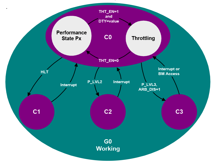
Fig. 8.1 Processor Power States
ACPI defines logic on a per-CPU basis that OSPM uses to transition between the different processor power states. This logic is optional, and is described through the FADT table and processor objects (contained in the hierarchical namespace). The fields and flags within the FADT table describe the symmetrical features of the hardware, and the processor object contains the location for the particular CPU’s clock logic (described by the P_BLK register block and _CST objects).
The P_LVL2 and P_LVL3 registers provide optional support for placing the system processors into the C2 or C3 states. The P_LVL2 register is used to sequence the selected processor into the C2 state, and the P_LVL3 register is used to sequence the selected processor into the C3 state. Additional support for the C3 state is provided through the bus master status and arbiter disable bits (BM_STS in the PM1_STS register and ARB_DIS in the PM2_CNT register). System software reads the P_LVL2 or P_LVL3 registers to enter the C2 or C3 power state. The Hardware must put the processor into the proper clock state precisely on the read operation to the appropriate P_LVLx register. The platform may alternatively define interfaces allowing OSPM to enter C-states using the _CST object, which is defined in _CST (C States).
Processor power state support is symmetric when presented via the FADT and P_BLK interfaces; OSPM assumes all processors in a system support the same power states. If processors have non-symmetric power state support, then the platform runtime firmware will choose and use the lowest common power states supported by all the processors in the system through the FADT table. For example, if the CPU0 processor supports all power states up to and including the C3 state, but the CPU1 processor only supports the C1 power state, then OSPM will only place idle processors into the C1 power state (CPU0 will never be put into the C2 or C3 power states). Notice that the C1 power state must be supported. The C2 and C3 power states are optional (see the PROC_C1 flag in the FADT table description in System Description Table Header).
The following sections describe processor power states in detail.
8.1.1. Processor Power State C0
While the processor is in the C0 power state, it executes instructions. While in the C0 power state, OSPM can generate a policy to run the processor at less than maximum performance. The clock throttling mechanism provides OSPM with the functionality to perform this task in addition to thermal control. The mechanism allows OSPM to program a value into a register that reduces the processor’s performance to a percentage of maximum performance.
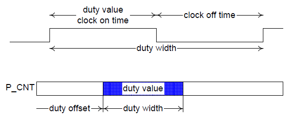
Fig. 8.2 Throttling Example
The FADT contains the duty offset and duty width values. The duty offset value determines the offset within the P_CNT register of the duty value. The duty width value determines the number of bits used by the duty value (which determines the granularity of the throttling logic). The performance of the processor by the clock logic can be expressed with the following equation:

Fig. 8.3 Equation 1 Duty Cycle Equation
Nominal performance is defined as “close as possible, but not below the indicated performance level.” OSPM will use the duty offset and duty width to determine how to access the duty setting field. OSPM will then program the duty setting based on the thermal condition and desired power of the processor object. OSPM calculates the nominal performance of the processor using the equation expressed in Equation 1. Notice that a dutysetting of zero is reserved.For example, the clock logic could use the stop grant cycle to emulate a divided processor clock frequency on an IA processor (through the use of the STPCLK# signal). This signal internally stops the processor’s clock when asserted LOW. To implement logic that provides eight levels of clock control, the STPCLK# pin could be asserted as follows (to emulate the different frequency settings):
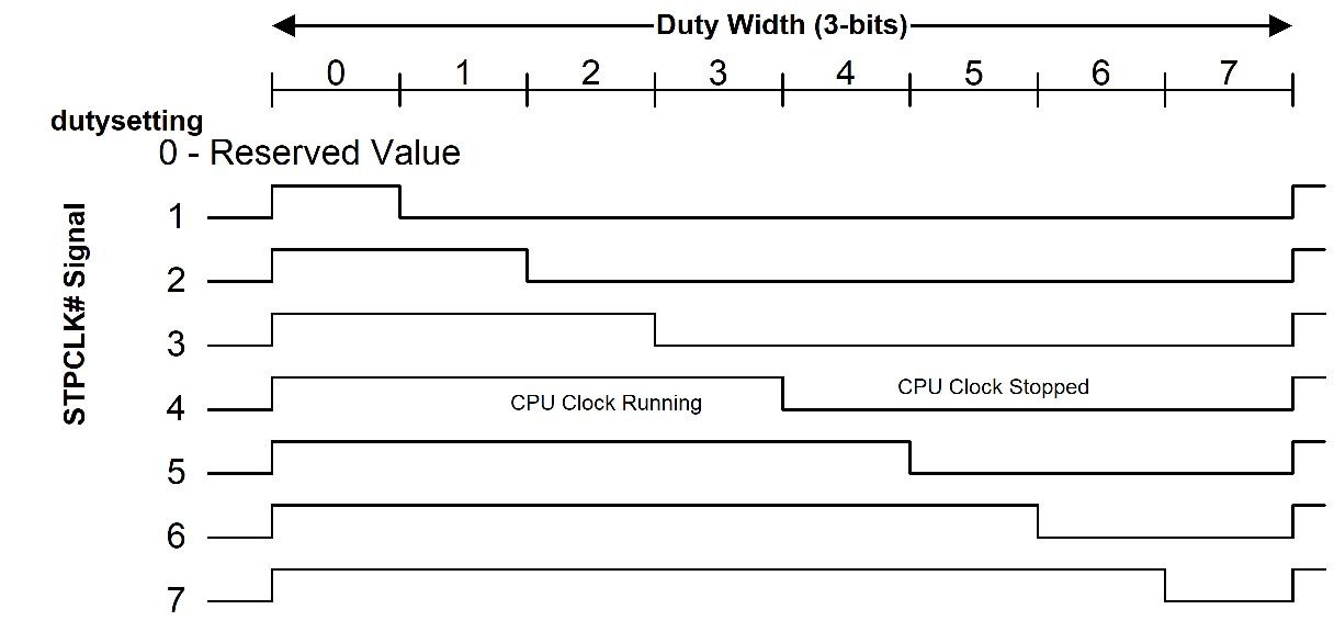
Fig. 8.4 Example Control for the STPCLK
To start the throttling logic OSPM sets the desired duty setting and then sets the THT_EN bit HIGH. To change the duty setting, OSPM will first reset the THT_EN bit LOW, then write another value to the duty setting field while preserving the other unused fields of this register, and then set the THT_EN bit HIGH again.
The example logic model is shown below:
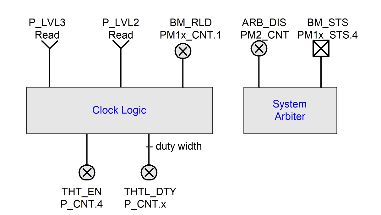
Fig. 8.5 ACPI Clock Logic (One per Processor)
Implementation of the ACPI processor power state controls minimally requires the support a single CPU sleeping state (C1). All of the CPU power states occur in the G0/S0 system state; they have no meaning when the system transitions into the sleeping state(S1-S4). ACPI defines the attributes (semantics) of the different CPU states (defines four of them). It is up to the platform implementation to map an appropriate low-power CPU state to the defined ACPI CPU state.
ACPI clock control is supported through the optional processor register block (P_BLK). ACPI requires that there be a unique processor register block for each CPU in the system. Additionally, ACPI requires that the clock logic for multiprocessor systems be symmetrical when using the P_BLK and FADT interfaces; if the P0 processor supports the C1, C2, and C3 states, but P1 only supports the C1 state, then OSPM will limit all processors to enter the C1 state when idle.
The following sections define the different ACPI CPU sleeping states.
8.1.2. Processor Power State C1
All processors must support this power state. This state is supported through a native instruction of the processor (HLT for IA 32-bit processors), and assumes no hardware support is needed from the chipset. The hardware latency of this state must be low enough that OSPM does not consider the latency aspect of the state when deciding whether to use it. Aside from putting the processor in a power state, this state has no other software-visible effects. In the C1 power state, the processor is able to maintain the context of the system caches.
The hardware can exit this state for any reason, but must always exit this state when an interrupt is to be presented to the processor.
8.1.3. Processor Power State C2
This processor power state is optionally supported by the system. If present, the state offers improved power savings over the C1 state and is entered by using the P_LVL2 command register for the local processor or an alternative mechanism as indicated by the _CST object. The worst-case hardware latency for this state is declared in the FADT and OSPM can use this information to determine when the C1 state should be used instead of the C2 state. Aside from putting the processor in a power state, this state has no other software-visible effects. OSPM assumes the C2 power state has lower power and higher exit latency than the C1 power state.
The C2 power state is an optional ACPI clock state that needs chipset hardware support. This clock logic consists of an interface that can be manipulated to cause the processor complex to precisely transition into a C2 power state. In a C2 power state, the processor is assumed capable of keeping its caches coherent; for example, bus master and multiprocessor activity can take place without corrupting cache context.
The C2 state puts the processor into a low-power state optimized around multiprocessor and bus master systems. OSPM will cause an idle processor complex to enter a C2 state if there are bus masters or Multiple processor activity (which will prevent OSPM from placing the processor complex into the C3 state). The processor complex is able to snoop bus master or multiprocessor CPU accesses to memory while in the C2 state.
The hardware can exit this state for any reason, but must always exit this state whenever an interrupt is to be presented to the processor.
8.1.4. Processor Power State C3
This processor power state is optionally supported by the system. If present, the state offers improved power savings over the C1 and C2 state and is entered by using the P_LVL3 command register for the local processor or an alternative mechanism as indicated by the _CST object. The worst-case hardware latency for this state is declared in the FADT, and OSPM can use this information to determine when the C1 or C2 state should be used instead of the C3 state. While in the C3 state, the processor’s caches maintain state but the processor is not required to snoop bus master or multiprocessor CPU accesses to memory.
The hardware can exit this state for any reason, but must always exit this state when an interrupt is to be presented to the processor or when BM_RLD is set and a bus master is attempting to gain access to memory.
OSPM is responsible for ensuring that the caches maintain coherency. In a uniprocessor environment, this can be done by using the PM2_CNT.ARB_DIS bus master arbitration disable register to ensure bus master cycles do not occur while in the C3 state. In a multiprocessor environment, the processors’ caches can be flushed and invalidated such that no dynamic information remains in the caches before entering the C3 state.
There are two mechanisms for supporting the C3 power state:
Having OSPM flush and invalidate the caches prior to entering the C3 state.
Providing hardware mechanisms to prevent masters from writing to memory (uniprocessor-only support).
In the first case, OSPM will flush the system caches prior to entering the C3 state. As there is normally much latency associated with flushing processor caches, OSPM is likely to only support this in multiprocessor platforms for idle processors. Flushing of the cache is accomplished through one of the defined ACPI mechanisms (described below in Flushing Caches).
In uniprocessor-only platforms that provide the needed hardware functionality (defined in this section), OSPM will attempt to place the platform into a mode that will prevent system bus masters from writing into memory while the processor is in the C3 state. This is accomplished by disabling bus masters prior to entering a C3 power state. Upon a bus master requesting an access, the CPU will awaken from the C3 state and re-enable bus master accesses.
OSPM uses the BM_STS bit to determine the power state to enter when considering a transition to or from the C2/C3 power state. The BM_STS is an optional bit that indicates when bus masters are active. OSPM uses this bit to determine the policy between the C2 and C3 power states: a lot of bus master activity demotes the CPU power state to the C2 (or C1 if C2 is not supported), no bus master activity promotes the CPU power state to the C3 power state. OSPM keeps a running history of the BM_STS bit to determine CPU power state policy.
The last hardware feature used in the C3 power state is the BM_RLD bit. This bit determines if the Cx power state is exited as a result of bus master requests. If set, then the Cx power state is exited upon a request from a bus master. If reset, the power state is not exited upon bus master requests. In the C3 state, bus master requests need to transition the CPU back to the C0 state (as the system is capable of maintaining cache coherency), but such a transition is not needed for the C2 state. OSPM can optionally set this bit when using a C3 power state, and clear it when using a C1 or C2 power state.
8.1.5. Additional Processor Power States
ACPI introduced optional processor power states beyond C3 starting in ACPI 2.0. These power states, C4… Cn, are conveyed to OSPM through the _CST object defined in _CST (C States) These additional power states are characterized by equivalent operational semantics to the C1 through C3 power states, as defined in the previous sections, but with different entry/exit latencies and power savings. See _CST (C States) for more information.