6. Device Configuration
This section specifies the objects OSPM uses to configure devices. There are three types of configuration objects:
Device identification objects associate platform devices with Plug and Play IDs.
Device configuration objects declare and configure hardware resources and characteristics for devices enumerated via ACPI.
Device insertion and removal objects provide mechanisms for handling dynamic insertion and removal of devices.
There are two types of Device objects:
A Full Device Descriptor, which contains the complete description of a devices that cannot be discovered through any other standard Bus enumeration mechanism. This type of Device object is enumerated by the ACPI subsystem (OSPM), and contains a Hardware ID object (_HID).
An Agumented Device Descriptor, which contains additional device information that is not provided from the Device itself, yet is needed by the Device or Bus driver in order to properly configure and use the device. This type of device is enumerated by a bus-specific enumeration mechanism, and OSPM uses the Address (_ADR) to match the ACPI Device object in the Namespace to the device discovered through bus enumeration.
This section also defines the ACPI device-resource descriptor formats. Device-resource descriptors are used as parameters by some of the device configuration objects.
6.1. Device Identification Objects
Device identification objects associate each platform device with a Plug and Play device ID for each device. All the device identification objects are listed in the table below:
Object |
Description |
|---|---|
_ADR |
Object that evaluates to a device’s address on its parent bus. |
_CID |
Object that evaluates to a device’s Plug and Play-compatible ID list. |
_CLS |
Object that evaluates to a package of coded device-class information. |
_DDN |
Object that associates a logical software name (for example, COM1) with a device. |
_HID |
Object that evaluates to a device’s Plug and Play hardware ID. |
_HRV |
Object that evaluates to an integer hardware revision number. |
_MLS |
Object that provides a human readable description of a device in multiple languages. |
_PLD |
Object that provides physical location description information. |
_SUB |
Object that evaluates to a device’s Plug and Play subsystem ID. |
_SUN |
Object that evaluates to the slot-unique ID number for a slot. |
_STR |
Object that contains a Unicode identifier for a device. Can also be used for thermal zones. |
_UID |
Object that specifies a device’s unique persistent ID, or a control method that generates it. |
For any device that is on a non-enumerable type of bus (for example, an ISA bus), OSPM enumerates the devices’ identifier(s) and the ACPI system firmware must supply an _HID object (plus one or more optional objects such as _CID, _CLS, _HRV, _SUB) for each device to enable OSPM to do that. For devices on an enumerable type of bus, such as a PCI bus, the ACPI system must identify which device on the enumerable bus is identified by a particular address; the ACPI system firmware must supply an _ADR object for each device to enable this. A device object must contain either an _HID object or an _ADR object, but must not contain both.
If any of these objects are implemented as control methods, these methods may depend on operation regions. Since the control methods may be evaluated before an operation region provider becomes available, the control method must be structured to execute in the absence of the operation region provider. (_REG methods notify the platform runtime firmware of the presence of operation region providers.) When a control method cannot determine the current state of the hardware due to a lack of operation region provider, it is recommended that the control method should return the condition that was true at the time that control passed from the platform boot firmware to the OS. (The control method should return a default, boot value).
6.1.1. _ADR (Address)
This object is used to supply OSPM with the address of a device on its parent bus. An _ADR object must be used when specifying the address of any device on a bus that has a standard enumeration algorithm (see Configuration and “Plug and Play”, for the situations when these devices do appear in the ACPI namespace). The _ADR object is valid only within an Augmented Device Descriptor.
Arguments:
None
Return Value:
An Integer containing the address of the device
An _ADR object can be used to provide capabilities to the specified address even if a device is not present. This allows the system to provide capabilities to a slot on the parent bus.
OSPM infers the parent bus and segment from the location of the _ADR object’s device package in the ACPI namespace. For more information about the positioning of device packages in the ACPI namespace, see Device (Declare Device Package)
_ADR object information must be static and can be defined for the following bus types listed in ADR Object Address Encodings.
BUS |
Address Encoding |
|---|---|
EISA |
EISA slot number 0-F |
Floppy Bus |
Drive select values used for programming the floppy controller to access the specified INT13 unit number. The _ADR Objects should be sorted based on drive select encoding from 0-3. |
I3C |
Bits [63:52] - Reserved Bits [51:48] - Master Instance Bits [47:0] - I3C Device Provisional ID, following encoding defined in the MIPI Specification for I3C. If an I3C device supports a static address instead of a Provisional ID, then bits [47:7] are Reserved (zero), and bits [6:0] are the 7-bit static address. |
IDE Controller |
0-Primary Channel, 1-Secondary Channel |
IDE Channel |
0-Master drive, 1-Slave drive |
Intel® High Definition Audio |
High word - SDI (Serial Data In) ID of the codec that contains the function group. Low word - Node ID of the function group. |
PCI |
High word-Device #, Low word-Function #. (for example, device 3, function 2 is 0x00030002). To refer to all the functions on a device #, use a function number of FFFF). |
PCMCIA |
Socket #; 0-First Socket |
PC CARD |
Socket #; 0-First Socket |
Serial ATA |
SATA Port: High word–Root port #, Low word–port number off of a SATA port multiplier, or 0xFFFF if no port multiplier attached. (For example, root port 2 would be 0x0002FFFF. If instead a port multiplier had been attached to root port 2, the ports connected to the multiplier would be encoded 0x00020000, 0x00020001, etc.) The value 0xFFFFFFFF is reserved. |
SMBus |
Lowest Slave Address |
USB Root HUB |
Only one child of the host controller. It must have an _ADR of 0. No other children or values of _ADR are allowed. |
USB Ports |
Port number (1-n) |
SDIO Bus |
High word - Slot number (0-First Slot) Low word - Function number (see SD specification for definitions.) |
NVDIMM |
NFIT Device handle as defined by the NVDIMM Region Mapping Structure |
6.1.2. _CID (Compatible ID)
This optional object is used to supply OSPM with a device’s Plug and Play-Compatible Device ID. Use _CID objects when a device has no other defined hardware standard method to report its compatible IDs. The _CID object is valid only within a Full Device Descriptor. An _HID object must also be present.
Arguments:
None
Return Value:
An Integer or String containing a single CID or a Package containing a list of CIDs
A _CID object evaluates to either:
A single Compatible Device ID
A package of Compatible Device IDs for the device – in the order of preference, highest preference first.
Each Compatible Device ID must be either:
A valid HID value (a 32-bit compressed EISA type ID or a string such as “ACPI0004”).
A string that uses a bus-specific nomenclature. For example, _CID can be used to specify the PCI ID. The format of a PCI ID string is one of the following:
"PCI\CC_ccss"
"PCI\CC_ccsspp"
"PCI\VEN_vvvv&DEV_dddd&SUBSYS_ssssssss&REV_rr"
"PCI\VEN_vvvv&DEV_dddd&SUBSYS_ssssssss"
"PCI\VEN_vvvv&DEV_dddd&REV_rr"
"PCI\VEN_vvvv&DEV_dddd"
Where:
cc       - hexadecimal representation of the Class Code byte
ss       - hexadecimal representation of the Subclass Code byte
pp       - hexadecimal representation of the Programming Interface byte
vvvv     - hexadecimal representation of the Vendor ID
dddd     - hexadecimal representation of the Device ID
ssssssss - hexadecimal representation of the Subsystem ID
rr       - hexadecimal representation of the Revision byte
A compatible ID retrieved from a _CID object is only meaningful if it is a non-NULL value.
Example ASL:
Device (XYZ) {
  Name (_HID, EISAID ("PNP0303")) // PC Keyboard Controller
  Name (_CID, EISAID ("PNP030B"))
}
6.1.3. _CLS (Class Code)
This object is used to supply OSPM with the PCI-defined base-class, sub-class and programming interface for a device. This object is optional. However, it may be useful for loading generic drivers on hardware that is compatible with PCI -defined device classes, but that is not implemented on the PCI bus (and is therefore enumerated by ACPI.)
Arguments:
None
Return Value:
A Package containing the PCI -defined class information as a list of Integers:
Package(3) {<base-class code>, <sub-class code>, <Programming Interface code>}
A list of available class codes and programming interface codes is provided by the PCI SIG. See “PCI Code and ID Assignment Specification”, available from “Links to ACPI-Related Documents” (http://uefi.org/acpi ) under the heading “PCI Code and ID Assignment Specification
Example ASL:
Device(SATA) //AHCI- compatible SATA controller
   {
   Name(_HID, "...")
   Name(_CLS, Package (3)
      {
      0x01, // Base Class (01h == Mass Storage)
      0x06, // Sub-Class (06h == SATA)
      0x01, // Programming Interface (01h == AHCI)
      })
   Name(_CRS, ResourceTemplate()
      {
      ... // AHCI-defined system resources
      })
   }
6.1.4. _DDN (DOS Device Name)
This object is used to associate a logical name (for example, COM1) with a device. This name can be used by applications to connect to the device.
Arguments:
None
Return Value:
A String containing the DOS device name
6.1.5. _HID (Hardware ID)
This object is used to supply OSPM with the device’s PNP ID or ACPI ID.
See also
PNP ID and ACPI ID Registry is at http://www.uefi.org/PNP_ACPI_Registry .
When describing a platform, use of any _HID objects is optional. However, a _HID object must be used to describe any device that will be enumerated by OSPM. OSPM only enumerates a device when no bus enumerator can detect the device ID. For example, devices on an ISA bus are enumerated by OSPM. Use the _ADR object to describe devices enumerated by bus enumerators other than OSPM. The _HID object is valid only within a Full Device Descriptor.
Arguments:
None
Return Value:
An Integer or String containing the HID
A _HID object evaluates to either a numeric 32-bit compressed EISA type ID or a string. If a string, the format must be an alphanumeric PNP or ACPI ID with no asterisk or other leading characters.
A valid PNP ID must be of the form “AAA####” where A is an uppercase letter and # is a hex digit. A valid ACPI ID must be of the form “NNNN####” where N is an uppercase letter or a digit (‘0’-‘9’) and # is a hex digit. This specification reserves the string “ACPI” for use only with devices defined herein. It further reserves all strings representing 4 HEX digits for exclusive use with PCI-assigned Vendor IDs.
Example ASL:
Name (_HID, EISAID ("PNP0C0C")) // Control-Method Power Button
Name (_HID, EISAID ("INT0800")) // Firmware Hub
Name (_HID, "ACPI0003") // AC adapter device
Name (_HID, "MSFT0003") // Vendor-defined device
Name (_HID, "80860003") // PCI-assigned device identifier
6.1.6. _HRV (Hardware Revision)
This object is used to supply OSPM with the device’s hardware revision. The use of _HRV is optional.
Arguments:
None
Return Value:
An Integer (DWORD) containing the hardware revision number
Example ASL:
Name (_HRV, 0x0003) // Revision number 3 of this hardware device
6.1.7. _MLS (Multiple Language String)
The _MLS object provides OSPM a human readable description of a device in multiple languages. This information may be provided to the end user when the OSPM is unable to get any other information about this device. Although this functionality is also provided by the _STR object, _MLS expands that functionality and provides vendors with the capability to provide multiple strings in multiple languages. The _MLS object evaluates to a package of packages. Each sub-package consists of a Language identifier and corresponding unicode string for a given locale. Specifying a language identifier allows OSPM to easily determine if support for displaying the Unicode string is available. OSPM can use this information to determine whether or not to display the device string, or which string is appropriate for a user’s preferred locale.
It is assumed that OSPM will always support the primary English locale to accommodate English embedded in a non-English string, such as a brand name.
If OSPM doesn’t support the specific sub-language ID it may choose to use the primary language ID for displaying device text.
Arguments:
None
Return Value:
A variable-length Package containing a list of language descriptor Packages as described below.
Return Value Information:
Package {
   LanguageDescriptor[0] // Package
   LanguageDescriptor[n] // Package
}
Each Language Descriptor sub-Package contains the elements described below:
Package {
   LanguageId // String
   UnicodeDescription // Buffer
}
LanguageId is a string identifying the language. This string follows the format specified in the Internet RFC 3066 document (Tags for the Identification of Languages). In addition to supporting the existing strings in RFC 3066, the table below lists aliases that are also supported.
RFC String |
Supported Alias String |
|---|---|
zh-Hans |
zh-chs |
zh-Hant |
zh-cht |
UnicodeDescription is a Buffer containing a Unicode (UTF-16) string. This string contains the language-specific description of the device corresponding to the LanguageID. The Unicode() ASL macro can be used to create this Buffer.
Example:
Device (XYZ) {
   Name (_ADR, 0x00020001)
   Name ( \_MLS, Package(){(2){"en", Unicode("ACME super DVD controller")}})
}
6.1.8. _PLD (Physical Location of Device)
This optional object is a method that conveys to OSPM a general description of the physical location of a device’s external connection point. The _PLD may be child object for any ACPI Namespace object the system wants to describe. This information can be used by system software to describe to the user which specific connector or device input mechanism may be used for a given task or may need user intervention for correct operation. The _PLD should only be evaluated when its parent device is present as indicated by the device’s presence mechanism (i.e. _STA or other)
An externally exposed device connection point can reside on any surface of a system’s housing. The respective surfaces of a system’s housing are identified by the “Panel” field (described below). The _PLD method returns data to describe the location of where the device’s connection point resides and a Shape (described below) that may be rendered at that position. One physical device may have several connection points. A _PLD describes the offset and rotation of a single device connection point from an “origin” that resides in the lower left hand corner of its Panel.
All Panel references (Top, Bottom, Right, Left, etc.) are interpreted as though the user is facing the front of the system. For handheld mobile devices, the front panel is the one holding the display screen, and its origin is in the lower-left corner when the display is viewed in the Portrait orientation. For example, the Right Panel is the right side of the system as viewed from the front.
All “origin” references for a Panel are interpreted as its lower left corner when the user is facing the respective Panel. The Top Panel shall be viewed with the system is viewed resting on its Front Panel, and the Bottom Panel shall be viewed with the system resting on its Back Panel. All other Panels shall be viewed with the system resting on its Bottom Panel. See System Panel and Panel Origin Positions for more information.
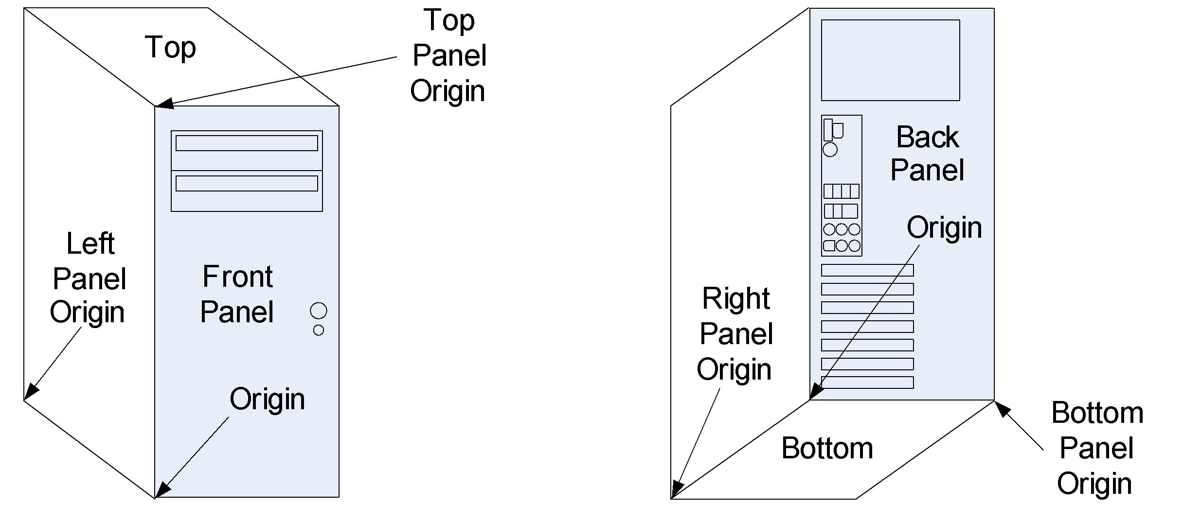
Fig. 6.1 System Panel and Panel Origin Positions
The data bits also assume that if the system is capable of opening up like a laptop that the device may exist on the base of the laptop system or on the lid. In the case of the latter, the “Lid” bit (described below) should be set indicating the device connection point is on the lid. If the device is on the lid, the description describes the device’s connection point location when the system is opened with the lid up. If the device connection point is not on the lid, then the description describes the device’s connection point location when the system with the lid closed.
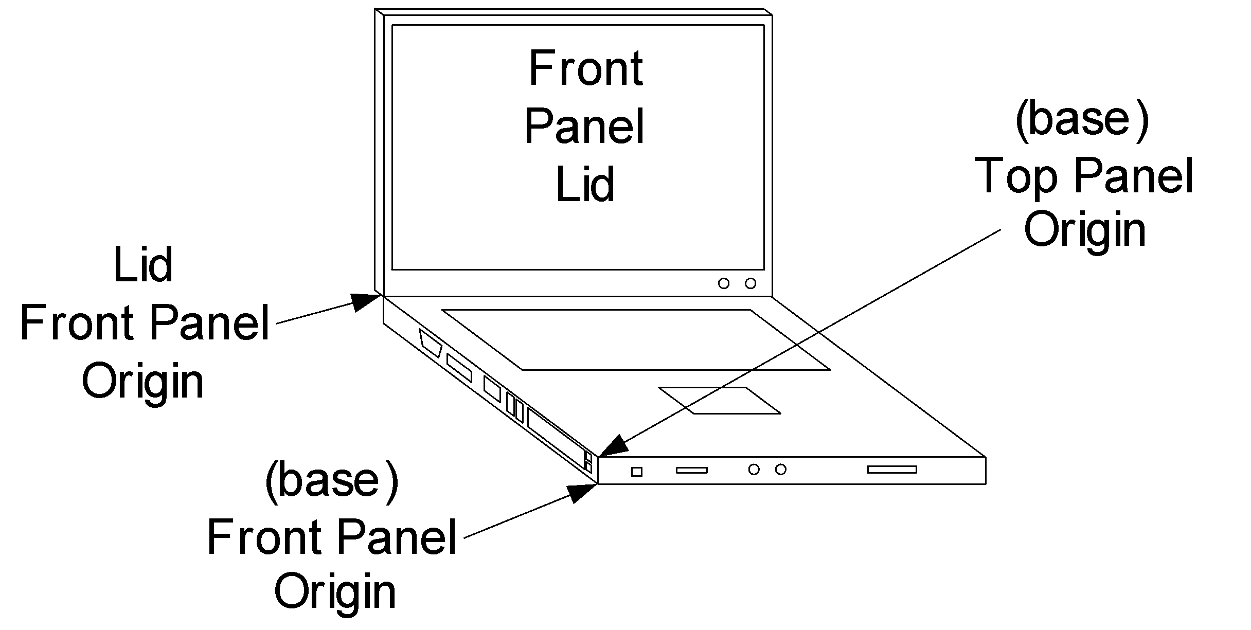
Fig. 6.2 Laptop Panel and Panel Origin Positions
To render a view of a system Panel, all _PLDs that define the same Panel and Lid values are collected. The _PLDs are then sorted by the value of their Order field and the view of the panel is rendered by drawing the shapes of each connection point (in their correct Shape, Color, Horizontal Offset, Vertical Offset, Width, Height, and Orientation) starting with all Order = 0 _PLDs first. Refer to PLD Back Panel Rendering for an example.
The location of a device connection point may change as a result of the system connecting or disconnecting to a docking station or a port replicator. As such, Notify event of type 0x09 will cause OSPM to re-evaluate the _PLD object residing under the particular device notified. If a platform is unable to detect the change of connecting or disconnecting to a docking station or port replicator, a _PLD object should not be used to describe the device connection points that will change location after such an event.
Arguments:
None
Return Value:
A variable-length Package containing a list of Buffers
This method returns a package containing a single or multiple buffer entries. At least one buffer entry must be returned using the bit definitions below.
Name |
Definition |
DWORD |
Bit Offset (DWORD) |
Bit Offset (Buffer) |
Length (bits) |
|---|---|---|---|---|---|
Revision |
The current Revision is 0x2 |
0 |
0 |
0 |
7 |
Ignore Color |
If this bit is set, the Color field is ignored, as the color is unknown. |
0 |
7 |
7 |
1 |
Color |
24-bit RGB value for the color of the device connection point:
Bits [15:8]=red value
Bits [23:16]=green value
Bits [31:24]=blue value
|
0 |
8 |
8 |
24 |
Width |
Width of the widest point of the device connection point, in millimeters |
1 |
0 |
32 |
16 |
Height |
Height of the tallest point of the device connection point, in millimeters |
1 |
16 |
48 |
16 |
User Visible |
Set if the device connection point can be seen by the user without disassembly. |
2 |
0 |
64 |
1 |
Dock |
Set if the device connection point resides in a docking station or port replicator. |
2 |
65 |
1 |
|
Lid |
Set if this device connection point resides on the lid of laptop system. |
2 |
66 |
1 |
|
Panel |
Describes which panel surface of the system’s housing the device connection point resides on:
0 - Top
1 - Bottom
2 - Left
3 - Right
4 - Front
5 - Back
6 - Unknown (Vertical Position and Horizontal Position will be ignored)
|
2 |
67 |
3 |
|
Vertical Position on the panel where the device connection point resides |
0 - Upper
1 - Center
2 - Lower
|
2 |
70 |
2 |
|
Horizontal Position on the panel where the device connection point resides. |
2 |
72 |
2 |
||
Shape |
Describes the shape of the device connection point. The Width and Height fields may be used to distort a shape, e.g. A Round shape will look like an Oval shape if the Width and Height are not equal. And a Vertical Rectangle or Horizontal Rectangle may look like a square if Width and Height are equal. See Default Shape Definitions:
0 - Round
1 - Oval
2 - Square
3 - Vertical Rectangle
4 - Horizontal Rectangle
5 - Vertical Trapezoid
6 - Horizontal Trapezoid
7 - Unknown - Shape rendered as a Rectangle with dotted lines
8 - Chamfered
15:9 - Reserved
|
2 |
74 |
4 |
|
Group Orientation |
if Set, indicates vertical grouping, otherwise horizontal is assumed. |
2 |
78 |
1 |
|
Group Token |
Unique numerical value identifying a group. |
2 |
79 |
1 |
|
Group Position |
Identifies this device connection point’s position in the group (i.e. 1st, 2nd) |
2 |
87 |
8 |
|
Bay |
Set if describing a device in a bay or if device connection point is a bay. |
2 |
95 |
1 |
|
Ejectable |
Set if the device is ejectable. Indicates ejectability in the absence of _EJx objects. |
2 |
96 |
1 |
|
OSPM Ejection required |
OSPM Ejection required: Set if OSPM needs to be involved with ejection process. User-operated physical hardware ejection is not possible. |
2 |
97 |
1 |
|
Cabinet Number |
For single cabinet system, this field is always 0. |
2 |
98 |
8 |
|
Card Cage Number |
For single card cage system, this field is always 0. |
2 |
106 |
8 |
|
Reference |
if Set, this _PLD defines a “reference” shape that is used to help orient the user with respect to the other shapes when rendering _PLDs. |
2 |
114 |
1 |
|
Rotation |
Rotates the Shape clockwise in 45 degree steps around its origin where:
0 - 0°
1 - 45°
2 - 90°
3 - 135°
4 - 180°
5 - 225°
6 - 270°
7 - 315°
|
2 |
115 |
4 |
|
Order |
Identifies the drawing order of the connection point described by a _PLD:
Order = 0 connection points are drawn before Order = 1 connection points.
Order = 1 before Order = 2, and so on.
Order = 31 connection points are drawn last.
Order should always start at 0 and be consecutively assigned.
|
2 |
119 |
5 |
|
Reserved |
Reserved, must contain a value of 0. |
2 |
124 |
4 |
|
Vertical Offset |
Offset of Shape Origin from Panel Origin (in mm). A value of 0xFFFFFFFF indicates that this field is not supplied. |
2 |
128 |
16 |
|
Horizontal Offset |
Offset of Shape Origin from Panel Origin (in mm). A value of 0xFFFFFFFF indicates that this field is not supplied. |
2 |
144 |
16 |
Note
All additional buffer entries returned may contain OEM-specific data, but must begin in a {GUID, data} pair. These additional data may provide complimentary physical location information specific to certain systems or class of machines.
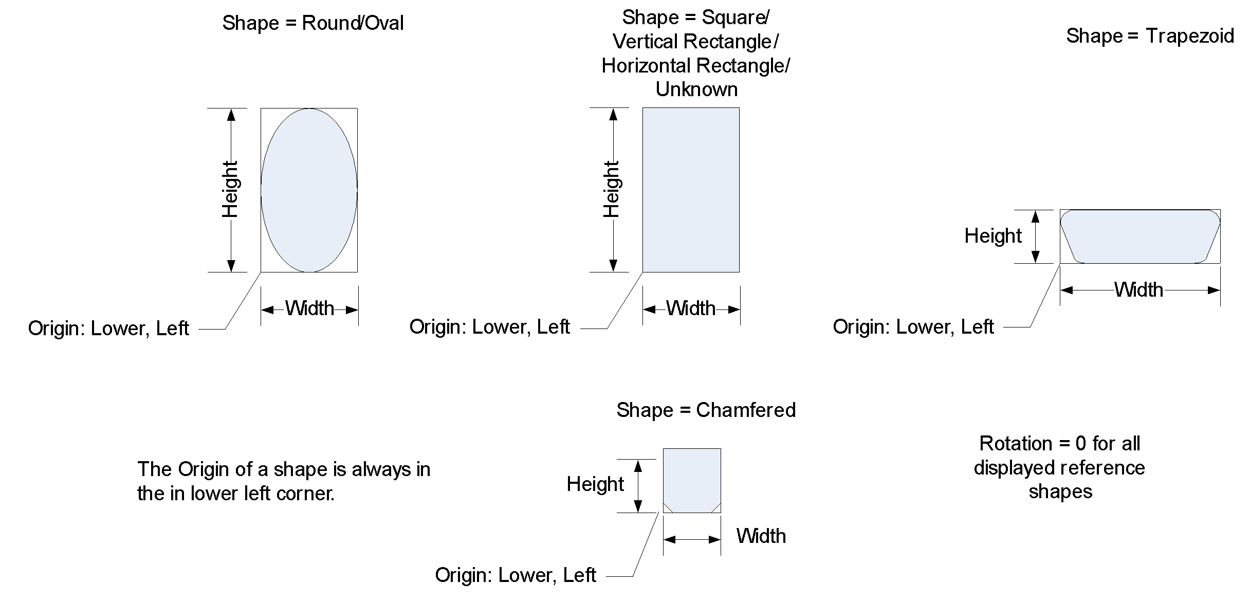
Fig. 6.3 Default Shape Definitions
Buffers 1–N Return Value (Optional):
Buffer 1 Bit [127:0] - GUID 1
Buffer 2 Bit [127:0] - Data 1
Buffer 3 Bit [127:0] - GUID 2
Buffer 4 Bit [127:0] - Data 2
etc.
PLD Back Panel Rendering provides an example of a rendering of the external device connection points that may be conveyed to the user by _PLD information. Note that three _PLDs (System Back Panel, Power Supply, and Motherboard (MB) Connector Area) that are associated with the System Bus tree (_SB) object. Their Reference flag is set indicating that are used to provide the user with visual queues for identifying the relative locations of the other device connection points.
The connection points (C1 through C16) are defined by _PLD objects found in the System bus tree.
The following connection points all have their Panel and Lid fields set to Back and 0, respectively. And the Reference flag of the System Back Panel, Power Supply, and MB Connector Area connection points are set to 1. in this example are used to render PLD Back Panel Rendering:
Name |
Ignore Color |
R |
G |
B |
Width |
Height |
VOff |
HOff |
Shape |
Notation |
Goup Position |
Rotation |
|---|---|---|---|---|---|---|---|---|---|---|---|---|
Back Panel |
Yes |
0 |
0 |
0 |
2032 |
4318 |
0 |
0 |
V Rect |
1 |
0 |
|
MB Conn area |
Yes |
0 |
0 |
0 |
445 |
1556 |
1588 |
127 |
V Rect |
2 |
0 |
|
Power Supply |
Yes |
0 |
0 |
0 |
1524 |
889 |
3302 |
127 |
H Rect |
2 |
0 |
|
USB Port 1 |
No |
0 |
0 |
0 |
125 |
52 |
2223 |
159 |
H Rect |
C1 |
3 |
90 |
USB Port 2 |
No |
0 |
0 |
0 |
125 |
52 |
2223 |
254 |
H Rect |
C2 |
3 |
90 |
USB Port 3 |
No |
0 |
0 |
0 |
125 |
52 |
2223 |
350 |
H Rect |
C3 |
3 |
90 |
USB Port 4 |
No |
0 |
0 |
0 |
125 |
52 |
2223 |
445 |
H Rect |
C4 |
3 |
90 |
USB Port 5 |
No |
0 |
0 |
0 |
125 |
52 |
2007 |
159 |
H Rect |
C5 |
3 |
90 |
USB Port 6 |
No |
0 |
0 |
0 |
125 |
52 |
2007 |
254 |
H Rect |
C6 |
3 |
90 |
Ethernet |
No |
0 |
0 |
0 |
157 |
171 |
2007 |
350 |
V Rect |
C7 |
3 |
90 |
Audio 1 |
No |
FF |
FF |
FF |
127 |
127 |
1945 |
151 |
Round |
C8 |
3 |
90 |
Audio 2 |
No |
151 |
247 |
127 |
127 |
127 |
1945 |
286 |
Round |
C9 |
3 |
90 |
Audio 3 |
No |
0 |
0 |
0 |
127 |
127 |
1945 |
427 |
Round |
C10 |
3 |
90 |
SPDIF |
No |
0 |
0 |
0 |
112 |
126 |
1756 |
176 |
V Trap |
C11 |
3 |
90 |
Audio 4 |
No |
0 |
FF |
0 |
127 |
127 |
1765 |
288 |
Round |
C12 |
3 |
90 |
Audio 5 |
No |
0 |
0 |
FF |
127 |
127 |
1765 |
429 |
Round |
C13 |
3 |
90 |
SATA |
No |
0 |
0 |
0 |
239 |
88 |
3091 |
159 |
H Rect |
C14 |
3 |
90 |
1394 |
No |
0 |
0 |
0 |
112 |
159 |
2890 |
254 |
H Trap |
C15 |
3 |
0 |
Coax |
No |
0 |
0 |
0 |
159 |
159 |
2842 |
143 |
Round |
C16 |
3 |
90 |
PCI 1 |
No |
0 |
0 |
0 |
1016 |
127 |
127 |
127 |
H Rect |
1 |
3 |
0 |
PCI 2 |
No |
0 |
0 |
0 |
1016 |
127 |
334 |
127 |
H Rect |
2 |
3 |
0 |
PCI 3 |
No |
0 |
0 |
0 |
1016 |
127 |
540 |
127 |
H Rect |
3 |
3 |
0 |
PCI 4 |
No |
0 |
0 |
0 |
1016 |
127 |
747 |
127 |
H Rect |
4 |
3 |
0 |
PCI 5 |
No |
0 |
0 |
0 |
1016 |
127 |
953 |
127 |
H Rect |
5 |
3 |
0 |
PCI 6 |
No |
0 |
0 |
0 |
1016 |
127 |
1159 |
127 |
H Rect |
6 |
3 |
0 |
PCI 7 |
No |
0 |
0 |
0 |
1016 |
127 |
1366 |
127 |
H Rect |
7 |
3 |
0 |
Note that the origin is in the lower left hand corner of the Back Panel, where positive Horizontal and Vertical Offset values are to the right and up, respectively.
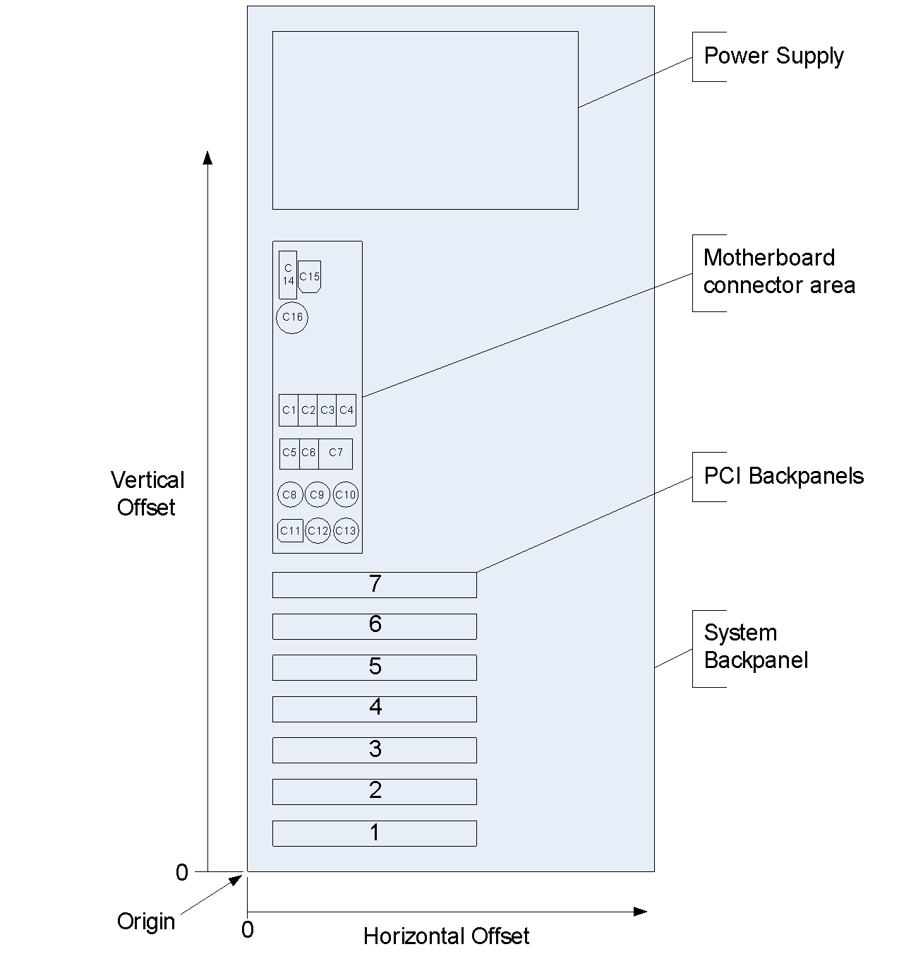
Fig. 6.4 PLD Back Panel Rendering
6.1.9. _SUB (Subsystem ID)
This object is used to supply OSPM with the device’s Subsystem ID. The use of _SUB is optional.
Arguments:
None
Return Value:
A String containing the SUB
A _SUB object evaluates to a string and the format must be a valid PNP or ACPI ID with no asterisk or other leading characters.
See the definition of _HID (_HID (Hardware ID) ) for the definition of PNP and ACPI ID strings.
Example ASL:
Name (_SUB, "MSFT3000") // Vendor-defined subsystem
6.1.10. _STR (String)
The _STR object evaluates to a Unicode string that describes the device or thermal zone. It may be used by an OS to provide information to an end user. This information is particularly valuable when no other information is available.
Arguments:
None
Return Value:
A Buffer containing a Unicode string that describes the device
Example ASL:
Device (XYZ) {
   Name (_ADR, 0x00020001)
   Name (_STR, Unicode ("ACME super DVD controller"))
}
Then, when all else fails, an OS can use the info included in the _STR object to describe the hardware to the user.
6.1.11. _SUN (Slot User Number)
_SUN is an object that evaluates to the slot-unique ID number for a slot. _SUN is used by OSPM UI to identify slots for the user. For example, this can be used for battery slots, PCI slots, PCMCIA slots, or swappable bay slots to inform the user of what devices are in each slot. _SUN evaluates to an integer that is the number to be used in the user interface.
Arguments:
None
Return Value:
An Integer containing the slot’s unique ID
The _SUN value is required to be unique among the slots of the same type. It is also recommended that this number match the slot number printed on the physical slot whenever possible.
6.1.12. _UID (Unique ID)
This object provides OSPM with a logical device ID that does not change across reboots. This object is optional, but is required when the device has no other way to report a persistent unique device ID. The _UID must be unique across all devices with either a common _HID or _CID. This is because a device needs to be uniquely identified to the OSPM, which may match on either a _HID or a _CID to identify the device. The uniqueness match must be true regardless of whether the OSPM uses the _HID or the _CID. OSPM typically uses the unique device ID to ensure that the device-specific information, such as network protocol binding information, is remembered for the device even if its relative location changes. For most integrated devices, this object contains a unique identifier.
In general, a _UID object evaluates to either a numeric value or a string. However, when defining an object with an _HID of ACPI0007 (processor definition objects), the _UID object must return an integer. This integer is used as an identifier in the MADT, PPTT and other tables to connect non-enumerable devices to a processor object. When a string is used in these cases, there is no mechanism for connecting these devices.
Arguments:
None
Return Value:
An Integer or String containing the Unique ID
6.2. Device Configuration Objects
This section describes objects that provide OSPM with device specific information and allow OSPM to configure device operation and resource utilization.
OSPM uses device configuration objects to configure hardware resources for devices enumerated via ACPI. Device configuration objects provide information about current and possible resource requirements, the relationship between shared resources, and methods for configuring hardware resources.
Note
these objects must only be provided for devices that cannot be configured by any other hardware standard such as PCI, PCMCIA, and soon.
When OSPM enumerates a device, it calls _PRS to determine the resource requirements of the device. It may also call _CRS to find the current resource settings for the device. Using this information, the Plug and Play system determines what resources the device should consume and sets those resources by calling the device’s _SRS control method.
In ACPI, devices can consume resources (for example, legacy keyboards), provide resources (for example, a proprietary PCI bridge), or do both. Unless otherwise specified, resources for a device are assumed to be taken from the nearest matching resource above the device in the device hierarchy.
Some resources, however, may be shared amongst several devices. To describe this, devices that share a resource (resource consumers) must use the extended resource descriptors (0x7-0xA) described in Large Resource Data Type. These descriptors point to a single device object (resource producer) that claims the shared resource in its _PRS. This allows OSPM to clearly understand the resource dependencies in the system and move all related devices together if it needs to change resources. Furthermore, it allows OSPM to allocate resources only to resource producers when devices that consume that resource appear.
The device configuration objects are listed in the table below.
Object |
Description |
|---|---|
_CCA |
Cache Coherency Attribute – specifies whether a device and its descendants support hardware managed cache coherency. |
_CDM |
Object that specifies a clock domain for a processor. |
_CRS |
Object that specifies a device’s current resource settings, or a control method that generates such an object. |
_DIS |
Control method that disables a device. |
_DMA |
Object that specifies a device’s current resources for DMA transactions. |
_DSD |
Object that evaluates to device specific information |
_FIX |
Object used to provide correlation between the fixed-hardware register blocks defined in the FADT and the devices that implement these fixed-hardware registers. |
_GSB |
Object that provides the Global System Interrupt Base for a hot-plugged I/O APIC device. |
_HMA |
Object that provides updated HMAT structures. |
_HPP |
Object that specifies the cache-line size, latency timer, SERR enable, and PERR enable values to be used when configuring a PCI device inserted into a hot-plug slot or initial configuration of a PCI device at system boot. |
_HPX |
Object that provides device parameters when configuring a PCI device inserted into a hot-plug slot or initial configuration of a PCI device at system boot. Supersedes _HPP. |
_MAT |
Object that evaluates to a buffer of Interrupt Controller Structures. |
_OSC |
An object OSPM evaluates to convey specific software support / capabilities to the platform allowing the platform to configure itself appropriately. |
_PRS |
An object that specifies a device’s possible resource settings, or a control method that generates such an object. |
_PRT |
Object that specifies the PCI interrupt routing table. |
_PXM |
Object that specifies a proximity domain for a device. |
_SLI |
Object that provides updated distance information for a system locality. |
_SRS |
Control method that sets a device’s settings. |
6.2.1. _CDM (Clock Domain)
This optional object conveys the processor clock domain to which a processor belongs. A processor clock domain is a unique identifier representing the hardware clock source providing the input clock for a given set of processors. This clock source drives software accessible internal counters, such as the Time Stamp Counter, in each processor. Processor counters in the same clock domain are driven by the same hardware clock source. In multi-processor platforms that utilize multiple clock domains, such counters may exhibit drift when compared against processor counters on different clock domains.
The _CDM object evaluates to an integer that identifies the device as belonging to a specific clock domain. OSPM assumes that two devices in the same clock domain are connected to the same hardware clock.
Arguments:
None
Return Value:
An Integer (DWORD) containing a clock domain identifier.
In the case the platform does not convey any clock domain information to OSPM via the SRAT or the _CDM object, OSPM assumes all logical processors to be on a common clock domain. If the platform defines _CDM object under a logical processor then it must define _CDM objects under all logical processors whose clock domain information is not provided via the SRAT.
6.2.2. _CRS (Current Resource Settings)
This required object evaluates to a byte stream that describes the system resources currently allocated to a device. Additionally, a bus device must supply the resources that it decodes and can assign to its children devices. If a device is disabled, then _CRS returns a valid resource template for the device, but the actual resource assignments in the return byte stream are ignored. If the device is disabled when _CRS is called, it must remain disabled.
The format of the data contained in a _CRS object follows the formats defined in Resource Data Types for ACPI, which is a compatible extension of the Plug and Play BIOS Specification (see reference below). The resource data is provided as a series of data structures, with each of the resource data structures having a unique tag or identifier. The resource descriptor data structures specify the standard PC system resources, such as memory address ranges, I/O ports, interrupts, and DMA channels.
See also
Plug and Play BIOS Specification Version 1.0A, May 5, 1994, Compaq Computer Corp., Intel Corp., Phoenix Technologies Ltd.
Arguments:
None
Return Value:
A Buffer containing a resource descriptor byte stream
6.2.3. _DIS (Disable)
This control method disables a device. When the device is disabled, it must not be decoding any hardware resources. Prior to running this control method, OSPM will have already put the device in the D3 state.
When a device is disabled via the _DIS, the _STA control method for this device must return with the Disabled bit set.
Arguments:
None
Return Value:
None
6.2.4. _DMA (Direct Memory Access)
This optional object returns a byte stream in the same format as a _CRS object. _DMA is only defined under devices that represent buses. It specifies the ranges the bus controller (bridge) decodes on the child-side of its interface. (This is analogous to the _CRS object, which describes the resources that the bus controller decodes on the parent-side of its interface.) Any ranges described in the resources of a _DMA object can be used by child devices for DMA or bus master transactions.
The _DMA object is only valid if a _CRS object is also defined. OSPM must re-evaluate the _DMA object after an _SRS object has been executed because the _DMA ranges resources may change depending on how the bridge has been configured.
If the _DMA object is not present for a bus device, the OS assumes that any address placed on a bus by a child device will be decoded either by a device on the bus or by the bus itself, (in other words, all address ranges can be used for DMA).
For example, if a platform implements a PCI bus that cannot access all of physical memory, it has a _DMA object under that PCI bus that describes the ranges of physical memory that can be accessed by devices on that bus.
A _DMA object is not meant to describe any “map register” hardware that is set up for each DMA transaction. It is meant only to describe the DMA properties of a bus that cannot be changed without reevaluating the _SRS method.
Arguments:
None
Return Value:
A Buffer containing a resource descriptor byte stream
_DMA Example ASL:
Device(BUS0)
{
   //
   // The _DMA method returns a resource template describing the
   // addresses that are decoded on the child side of this
   // bridge. The contained resource descriptors thus indicate
   // the address ranges that bus masters living below this
   // bridge can use to send accesses through the bridge toward a
   // destination elsewhere in the system (e.g. main memory).
   //
   // In our case, any bus master addresses need to fall between
   // 0 and 0x80000000 and will have 0x200000000 added as they
   // cross the bridge. Furthermore, any child-side accesses
   // falling into the range claimed in our _CRS will be
   // interpreted as a peer-to-peer traffic and will not be
   // forwarded upstream by the bridge.
   //
   // Our upstream address decoder will only claim one range from
   // 0x20000000 to 0x5fffffff in the _CRS. Therefore _DMA
   // should return two QWORDMemory descriptors, one describing
   // the range below and one describing the range above this
   // "peer-to-peer" address range.
   //
Method(_DMA, ResourceTemplate()
{
   QWORDMemory(
      ResourceConsumer,
      PosDecode, // _DEC
      MinFixed, // _MIF
      MaxFixed, // _MAF
      Prefetchable, // _MEM
      ReadWrite, // _RW
      0, // _GRA
      0, // _MIN
      0x1fffffff, // _MAX
      0x200000000, // _TRA
      0x20000000, // _LEN
      ,
      ,
      ,
   )
   QWORDMemory(
      ResourceConsumer,
      PosDecode, // _DEC
      MinFixed, // _MIF
      MaxFixed, // _MAF
      Prefetchable, // _MEM
      ReadWrite, // _RW
      0, // _GRA
      0x60000000, // _MIN
      0x7fffffff, // _MAX
      0x200000000, // _TRA
      0x20000000, // _LEN
      ,
      ,
      ,
   )
 })
}
6.2.5. _DSD (Device Specific Data)
This optional object is used to provide device drivers (via OSPM) with additional device properties and information. _DSD returns a variable-length package containing a list of Device Data Descriptor structures each consisting of a UUID (see Universally Unique Identifiers (UUIDs)) and a package (Data Structure). The UUID is all that is needed to define the Data Structure. The UUID itself may place a restriction based on _HID or the optional _CID, _CLS, _HRV, _SUB objects, or _HID and one of those optional objects. However, it also may not place such a restriction.
New UUIDs may be created by OEMs and IHVs or other interface or device governing bodies (e.g. the PCI SIG or the UEFI Forum), as long as the UUID is different from other published UUIDs.
The list of well-known UUIDs allocated for _DSD and the definition of data formats associated with them is available in an auxiliary document hosted on the UEFI Forum: http://www.uefi.org/acpi .
Arguments:
None
Return Value:
A variable-length Package containing a list of Device Data Descriptor structures as described below.
Return Value Information:
Package ()
{
    Device Data Descriptor 0
    ...
    Device Data Descriptor n
}
Each Device Data Descriptor structure consists of two elements, as follows:
UUID            // Buffer (16 bytes)
Data Structure  // Package (depending on UUID)
UUID uniquely determines the format of Data Structure.
Data Structure is a set of device specific data items the format of which is uniquely determined by the UUID and the meaning of which is uniquely determined by the UUID possibly in combination with a PNP or ACPI device ID.
Multiple Device Data Descriptor structures with the same UUID are not permitted.
_DSD must return the same data each time it is evaluated. Firmware should not expect it to be evaluated every time (in case it is implemented as a method).
Examples:
Note
The UUID used in the following examples is assumed to define the data format for Data Structure as a list of packages of length 2 (Properties) whose first element (Key) must be a String and the second element is a Value associated with that key. The set of valid Keys and the format and interpretation of the Values associated with them is then dependent on the PNP or ACPI device ID of the device.
Device (MDEV) {
Name (_HID, "PNP####")

Name (_DSD, Package () {
        ToUUID("daffd814-6eba-4d8c-8a91-bc9bbf4aa301"),
        Package () {
            Package (2) {...}, // Property 1
            ...
            Package (2) {...} // Property n
        }
    })
}

//
// PWM controller with two pins that can be driven and a device using
// those pins with the periods of 5000000 and 4500000 nanoseconds,
// respectively.
//
Device (\_SB.PCI0.PWM) {
    Name (_HID, "PNP####")

    Name (_DSD, Package () {
        ToUUID("daffd814-6eba-4d8c-8a91-bc9bbf4aa301"),
        Package () {
            Package (2) {"#pwm-cells", 2}
        }
    })
}
Device (\_SB.PCI0.BL) {
    Name (_HID, "ACPI####")

    Name (_DSD, Package () {
        ToUUID("daffd814-6eba-4d8c-8a91-bc9bbf4aa301"),
        Package () {
            Package (2) {
                "pwms",
                Package () {
                \_SB.PCI0.PWM, 0, 5000000,
                \_SB.PCI0.PWM, 1, 4500000
                }
            }
        }
    })
}
//
// SPI controller using a fixed frequency clock represented by the CLKO
// device object.
//
Device (\_SB_.PCI0) {
    Device (CLK0) {
        Name (_HID, "PNP####")

        Name (_DSD, Package () {
            ToUUID("daffd814-6eba-4d8c-8a91-bc9bbf4aa301"),
            Package () {
                Package (2) {"#clock-cells", 0},
                Package (2) {"clock-frequency", 120000000}
            }
        })
    }

    Device (SPI0) {
        Name (_HID, "PNP####")

        Name (_DSD, Package () {
            ToUUID("daffd814-6eba-4d8c-8a91-bc9bbf4aa301"),
            Package () {
                Package (2) {"clocks", Package () {1, ^CLK0}}
            }
        })

        ...
    }
}
6.2.6. _FIX (Fixed Register Resource Provider)
This optional object is used to provide a correlation between the fixed-hardware register blocks defined in the FADT and the devices in the ACPI namespace that implement these fixed-hardware registers. This object evaluates to a package of Plug and Play-compatible IDs (32-bit compressed EISA type IDs) that correlate to the fixed-hardware register blocks defined in the FADT. The device under which _FIX appears plays a role in the implementation of the fixed-hardware (for example, implements the hardware or decodes the hardware’s address). _FIX conveys to OSPM whether a given device can be disabled, powered off, or should be treated specially by conveying its role in the implementation of the ACPI fixed-hardware register interfaces. This object takes no arguments.
The _CRS object describes a device’s resources. That _CRS object may contain a superset of the resources in the FADT, as the device may actually decode resources beyond what the FADT requires. Furthermore, in a machine that performs translation of resources within I/O bridges, the processor-relative resources in the FADT may not be the same as the bus-relative resources in the _CRS.
Arguments:
None
Return Value:
A variable-length Package containing a list of Integers, each containing a PNP ID
Each of fields in the FADT has its own corresponding Plug and Play ID, as shown below:
PNP0C20 - SMI_CMD
PNP0C21 - PM1a_EVT_BLK / X\_ PM1a_EVT_BLK
PNP0C22 - PM1b_EVT_BLK / X_PM1b_EVT_BLK
PNP0C23 - PM1a_CNT_BLK / X_PM1a_CNT_BLK
PNP0C24 - PM1b_CNT_BLK / X\_ PM1b_CNT_BLK
PNP0C25 - PM2_CNT_BLK / X\_ PM2_CNT_BLK
PNP0C26 - PM_TMR_BLK / X\_ PM_TMR_BLK
PNP0C27 - GPE0_BLK / X_GPE0_BLK
PNP0C28 - GPE1_BLK / X\_ GPE1_BLK
PNP0B00 - FIXED_RTC
PNP0B01 - FIXED_RTC
PNP0B02 - FIXED_RTC
Example ASL for _FIX usage:
Scope(\_SB) {
    Device(PCI0) {                      // Root PCI Bus
        Name(_HID, EISAID("PNP0A03"))   // Need \_HID for root device
        Method (_CRS,0){                // Need current resources for root device
                                        // Return current resources for root bridge 0
        }
        Name(_PRT, Package(){           // Need PCI IRQ routing for PCI bridge
                                        // Package with PCI IRQ routing table information
        })
        Name(_FIX, Package(1) {
            EISAID("PNP0C25")}           // PM2 control ID
        )
        Device (PX40) {                 // ISA
            Name(_ADR,0x00070000)
            Name(_FIX, Package(1) {
                EISAID("PNP0C20")}      // SMI command port
            )
            Device (NS17) {              // NS17 (Nat. Semi 317, an ACPI part)
                Name(_HID, EISAID("PNP0C02"))
                Name(_FIX, Package(3) {
                    EISAID("PNP0C22"),  // PM1b event ID
                    EISAID("PNP0C24"),  // PM1b control ID
                    EISAID("PNP0C28")}  // GPE1 ID
            }
        }                               // end PX40
        Device (PX43) {                 // PM Control
            Name(_ADR,0x00070003)
            Name(_FIX, Package(4) {
                EISAID("PNP0C21"),      // PM1a event ID
                EISAID("PNP0C23"),      // PM1a control ID
                EISAID("PNP0C26"),      // PM Timer ID
                EISAID("PNP0C27")}      // GPE0 ID
            )
        }                               // end PX43
    }                                   // end PCI0
}                                       // end scope SB
6.2.7. _GSB (Global System Interrupt Base)
_GSB is an optional object that evaluates to an integer that corresponds to the Global System Interrupt Base for the corresponding I/O APIC device. The I/O APIC device may either be bus enumerated (e.g. as a PCI device) or enumerated in the namespace as described in I/O APIC Device. Any I/O APIC device that either supports hot-plug or is not described in the MADT must contain a _GSB object.
If the I/O APIC device also contains a _MAT object, OSPM evaluates the _GSB object first before evaluating the _MAT object. By providing the Global System Interrupt Base of the I/O APIC, this object enables OSPM to process only the _MAT entries that correspond to the I/O APIC device. See _MAT (Multiple APIC Table Entry). Since _MAT is allowed to potentially return all the MADT entries for the entire platform, _GSB is needed in the I/O APIC device scope to enable OSPM to identify the entries that correspond to that device.
If an I/O APIC device is activated by a device-specific driver, the physical address used to access the I/O APIC will be exposed by the driver and cannot be determined from the _MAT object. In this case, OSPM cannot use the _MAT object to determine the Global System Interrupt Base corresponding to the I/O APIC device and hence requires the _GSB object.
The Global System Interrupt Base is a 64-bit value representing the corresponding I/OAPIC device as defined in Global System Interrupts.
Arguments:
None Return Value: An Integer containing the interrupt base
Example ASL for _GSB usage for a non-PCI based I/O APIC Device:
Scope(\_SB) {
    ...
    Device(APIC) { // I/O APIC Device
        Name(_HID, "ACPI0009") // ACPI ID for I/O APIC
    Name(_CRS, ResourceTemplate()
            { ...}) // only one resource pointing to I/O APIC register base
    Method(_GSB){
        Return (0x10) // Global System Interrupt Base for I/O APIC starts at 16
        }
    } // end APIC
} // end scope SB
Example ASL for _GSB usage for a PCI-based I/O APIC Device:
Scope(\_SB) {
    Device(PCI0) // Host bridge
        Name(_HID, EISAID("PNP0A03"))   // Need \_HID for root device
        Device(PCI1) { // I/O APIC PCI Device
            Name(_ADR,0x00070000)
    Method(_GSB){
        Return (0x18)                   // Global System Interrupt Base for I/O APIC starts at 24
        }
      }                                 // end PCI1
    }                                   // end PCI0
}                                       // end scope SB
6.2.8. _HPP (Hot Plug Parameters)
This optional object evaluates to a package containing the cache-line size, latency timer, SERR enable, and PERR enable values to be used when configuring a PCI device inserted into a hot-plug slot or for performing configuration of a PCI devices not configured by the platform boot firmware at system boot. The object is placed under a PCI bus where this behavior is desired, such as a bus with hot-plug slots. _HPP provided settings apply to all child buses, until another _HPP object is encountered.
Arguments:
None
Return Value:
A Package containing the Integer hot-plug parameters
Example:
Method (_HPP, 0) {
    Return (Package(4){
        0x08, // CacheLineSize in DWORDS
        0x40, // LatencyTimer in PCI clocks
        0x01, // Enable SERR (Boolean)
        0x00 // Enable PERR (Boolean)
    })
}
Field |
Object Type |
Definition |
|---|---|---|
Cache-line size |
Integer |
Cache-line size reported in number of DWORDs. |
Latency timer |
Integer |
Latency timer value reported in number of PCI clock cycles. |
Enable SERR |
Integer |
When set to 1, indicates that action must be performed to enable SERR in the command register. |
Enable PERR |
Integer |
When set to 1, indicates that action must be performed to enable PERR in the command register. |
Example: Using _HPP
Scope(\_SB) {
    Device(PCI0) { // Root PCI Bus
        Name(_HID, EISAID("PNP0A03"))   // \_HID for root device
        Method (_CRS,0){           // Need current resources for root dev
                                   // Return current resources for root bridge 0
        }
        Name(_PRT, Package(){      // Need PCI IRQ routing for PCI bridge
                                   // Package with PCI IRQ routing table information
        })
        Device (P2P1) { // First PCI-to-PCI bridge (No Hot Plug slots)
            Name(_ADR,0x000C0000)  // Device#Ch, Func#0 on bus PCI0
            Name(_PRT, Package(){  // Need PCI IRQ routing for PCI bridge
                                   // Package with PCI IRQ routing table information
        })
    }                              // end P2P1
        Device (P2P2) {
                                   // Second PCI-to-PCI bridge (Bus contains Hot plug slots)
            Name(_ADR,0x000E0000)  // Device#Eh, Func#0 on bus PCI0
            Name(_PRT, Package(){  // Need PCI IRQ routing for PCI bridge
                                   // Package with PCI IRQ routing table information
            })
            Name(_HPP, Package(){0x08,0x40, 0x01, 0x00})
            // Device definitions for Slot 1- HOT PLUG SLOT
            Device (S1F0) {        // Slot 1, Func#0 on bus P2P2
                Name(_ADR,0x00020000)
                Method(_EJ0, 1) {  // Remove all power to device}
            }
            Device (S1F1) {        // Slot 1, Func#1 on bus P2P2
                Name(_ADR,0x00020001)
                Method(_EJ0, 1) {  // Remove all power to device}
            }
            Device (S1F2) {        // Slot 1, Func#2 on bus P2P2
                Name(_ADR,0x000200 02)
                Method(_EJ0, 1) {  // Remove all power to device}
            }
            Device (S1F3) {        // Slot 1, Func#3 on bus P2P2
                Name(_ADR,0x00020003)
                Method(_EJ0, 1) {  // Remove all power to device}
            }
            Device (S1F4) {        // Slot 1, Func#4 on bus P2P2
                Name(_ADR,0x00020004)
                Method(_EJ0, 1) {  // Remove all power to device}
            }
            Device (S1F5) {        // Slot 1, Func#5 on bus P2P2
                Name(_ADR,0x00020005)
                Method(_EJ0, 1) {  // Remove all power to device}
            }
            Device (S1F6) {        // Slot 1, Func#6 on bus P2P2
                Name(_ADR,0x00020006)
                Method(_EJ0, 1) {  // Remove all power to device}
            }
            Device (S1F7) {        // Slot 1, Func#7 on bus P2P2
                Name(_ADR,0x00020007)
                Method(_EJ0, 1) {  // Remove all power to device}
            }
            // Device definitions for Slot 2- HOT PLUG SLOT
            Device (S2F0) {        // Slot 2, Func#0 on bus P2P2
                Name(_ADR,0x00030000)
                Method(_EJ0, 1) {  // Remove all power to device}
            }
            Device (S2F1) {        // Slot 2, Func#1 on bus P2P2
                Name(_ADR,0x00030001)
                Method(_EJ0, 1) {  // Remove all power to device}
            }
            Device (S2F2) {        // Slot 2, Func#2 on bus P2P2
                Name(_ADR,0x00030002)
                Method(_EJ0, 1) {  // Remove all power to device}
            }
            Device (S2F3) {        // Slot 2, Func#3 on bus P2P2
                Name(_ADR,0x00030003)
                Method(_EJ0, 1) {  // Remove all power to device}
            }
            Device (S2F4) {        // Slot 2, Func#4 on bus P2P2
                Name(_ADR,0x00030004)
                Method(_EJ0, 1) {  // Remove all power to device}
            }
            Device (S2F5) {        // Slot 2, Func#5 on bus P2P2
                Name(_ADR,0x00030005)
                Method(_EJ0, 1) {  // Remove all power to device}
            }
            Device (S2F6) {        // Slot 2, Func#6 on bus P2P2
                Name(_ADR,0x00030006)
                Method(_EJ0, 1) {  // Remove all power to device}
            }
            Device (S2F7) {        // Slot 2, Func#7 on bus P2P2
                Name(_ADR,0x00030007)
                Method(_EJ0, 1) {  // Remove all power to device}
            }
        }                          // end P2P2
    }                              // end PCI0
}                                  // end Scope (\_SB)
OSPM will configure a PCI device on a card hot-plugged into slot 1 or slot 2, with a cache line size of 32 (Notice this field is in DWORDs), latency timer of 64, enable SERR, but leave PERR alone.
6.2.9. _HPX (Hot Plug Parameter Extensions)
This optional object provides platform-specific information to the OSPM PCI driver component responsible for configuring PCI, PCI-X, or PCI Express Functions. The information conveyed applies to the entire hierarchy downward from the scope containing the _HPX object. If another _HPX object is encountered downstream, the settings conveyed by the lower-level object apply to that scope downward.
OSPM uses the information returned by _HPX to determine how to configure PCI Functions that are hot-plugged into the system, to configure Functions not configured by the platform firmware during initial system boot, and to configure Functions any time they lose configuration space settings (e.g. OSPM issues a Secondary Bus Reset/Function Level Reset or Downstream Port Containment is triggered). The _HPX object is placed within the scope of a PCI-compatible bus where this behavior is desired, such as a bus with hot-plug slots. It returns a single package that contains one or more sub-packages, each containing a single Setting Record. Each such Setting Record contains a Setting Type (INTEGER), a Revision number (INTEGER) and type/revision specific contents.
The format of data returned by the _HPX object is extensible. The Setting Type and Revision number determine the format of the Setting Record. OSPM ignores Setting Records of types that it does not understand. A Setting Record with higher Revision number supersedes that with lower revision number, however, the _HPX method can return both together, OSPM shall use the one with highest revision number that it understands. Type 3 records may have multiple records with the same revision or different revision (refer to the Revision field in PCI Express Descriptor Setting Record Content. Out of all the Type 3 records, the OSPM shall determine the highest revision number that it understands and use all Type 3 records with that revision.
_HPX may return multiple types or Record Settings (each setting in a single sub-package.) OSPM is responsible for detecting the type of Function and for applying the appropriate settings. OSPM is also responsible for detecting the device / port type of the PCI Express Function and applying the appropriate settings provided. For example, the Secondary Uncorrectable Error Severity and Secondary Uncorrectable Error Mask settings of Type 2 record are only applicable to PCI Express to PCI-X/PCI Bridge whose device / port type is 1000b. Similarly, AER settings are only applicable to hot plug PCI Express devices that support the optional AER capability.
Arguments:
None
Return Value:
A variable-length Package containing a list of Packages, each containing a single PCI, PCI-X, PCI Express, or PCI Express Descriptor Record Setting as described below
The _HPX object supersedes the _HPP object. If the _HPP and _HPX objects exist within a device’s scope, OSPM will only evaluate the _HPX object.
Note
OSPM may override the settings provided by the _HPX object’s Type2 record (PCI Express Settings) or Type3 record (PCI Express Descriptor Settings) when OSPM has assumed native control of the corresponding feature. For example, if OSPM has assumed ownership of AER (via _OSC), OSPM may override AER related settings returned by _HPX.
Note
Since error status registers do not drive error signaling, OSPM is not required to clear error status registers as part of _HPX handling.
Note
There are other mechanisms besides _HPX that provide platform-specific information to the OSPM PCI driver component responsible for configuring PCI, PCI-X, or PCI Express Functions (e.g., _DSM Definitions for Latency Tolerance Reporting as defined in the PCI Firmware Specification). System firmware should only provide platform-specific information via one of these mechanisms for any given register or feature (i.e., if Latency Tolerance Reporting information is provided via _DSM Definitions for Latency Tolerance Reporting then no information related to Latency Tolerance Reporting should be provided by _HPX and vice versa). Failure to do so will result in undefined behavior from the OSPM.
6.2.9.1. PCI Setting Record (Type 0)
The PCI setting record contains the setting type 0, the current revision 1 and the type/revision specific content: cache-line size, latency timer, SERR enable, and PERR enable values.
Field |
Object Type |
Definition |
|---|---|---|
Header |
||
- Type |
Integer |
0x00: Type 0 (PCI) setting record. |
- Revision |
Integer |
0x01: Revision 1, defining the set of fields below. |
Cache-line size |
Integer |
Cache-line size reported in number of DWORDs. |
Latency timer |
Integer |
Latency timer value reported in number of PCI clock cycles. |
Enable SERR |
Integer |
When set to 1, indicates that action must be performed to enable SERR in the command register. |
Enable PERR |
Integer |
When set to 1, indicates that action must be performed to enable PERR in the command register. |
If the hot plug device includes bridge(s) in the hierarchy, the above settings apply to the primary side (command register) of the hot plugged bridge(s). The settings for the secondary side of the bridge(s) (Bridge Control Register) are assumed to be provided by the bridge driver.
The Type 0 record is applicable to hot plugged PCI, PCI-X and PCI Express devices. OSPM will ignore settings provided in the Type0 record that are not applicable (for example, Cache-line size and Latency Timer are not applicable to PCI Express).
6.2.9.2. PCI-X Setting Record (Type 1)
The PCI-X setting record contains the setting type 1, the current revision 1 and the type/revision specific content: the maximum memory read byte count setting, the average maximum outstanding split transactions setting and the total maximum outstanding split transactions to be used when configuring PCI-X command registers for PCI-X buses and/or devices.
Field |
Object Type |
Definition |
|---|---|---|
Header |
||
- Type |
Integer |
0x01: Type 1 (PCI-X) setting record. |
- Revision |
Integer |
0x01: Revision 1, defining the set of fields below. |
Maximum memory read byte count |
Integer |
Maximum memory read byte count reported: Value 0: Maximum byte count 512 Value 1: Maximum byte count 1024 Value 2: Maximum byte count 2048 Value 3: Maximum byte count 4096 |
Average maximum outstanding split transactions |
Integer |
The following values are defined: Value 0: Maximum outstanding split transaction 1 Value 1: Maximum outstanding split transaction 2 Value 2: Maximum outstanding split transaction 3 Value 3: Maximum outstanding split transaction 4 Value 4: Maximum outstanding split transaction 8 Value 5: Maximum outstanding split transaction 12 Value 6: Maximum outstanding split transaction 16 Value 7: Maximum outstanding split transaction 32 |
Total maximum outstanding split transactions |
Integer |
See the definition for the average maximum outstanding split transactions. |
For simplicity, OSPM could use the Average Maximum Outstanding Split Transactions value as the Maximum Outstanding Split Transactions register value in the PCI-X command register for each PCI-X device. Another alternative is to use a more sophisticated policy and the Total Maximum Outstanding Split Transactions Value to gain even more performance. In this case, the OS would examined each PCI-X device that is directly attached to the host bridge, determine the number of outstanding split transactions supported by each device, and configure each device accordingly. The goal is to ensure that the aggregate number of concurrent outstanding split transactions does not exceed the Total Maximum Outstanding Split Transactions Value: an integer denoting the number of concurrent outstanding split transactions the host bridge can support (the minimum value is 1).
This object does not address providing additional information that would be used to configure registers in bridge devices, whether architecturally-defined or specification-defined registers or device specific registers. It is expected that a driver for a bridge would be the proper implementation mechanism to address both of those issues. However, such a bridge driver should have access to the data returned by the _HPX object for use in optimizing its decisions on how to configure the bridge. Configuration of a bridge is dependent on both system specific information such as that provided by the _HPX object, as well as bridge specific information.
6.2.9.3. PCI Express Setting Record (Type 2)
The PCI Express setting record contains the setting type 2, the current revision 1 and the type/revision specific content (the control registers as listed in the table below) to be used when configuring registers in the Advanced Error Reporting Extended Capability Structure or PCI Express Capability Structure for the PCI Express devices.
The Type 2 Setting Record allows a PCI Express-aware OS that supports native hot plug to configure the specified registers of the hot plugged PCI Express device. A PCI Express-aware OS that has assumed ownership of native hot plug (via _OSC) but does not support or does not have ownership of the AER register set must use the data values returned by the _HPX object’s Type 2 record to program the AER registers of a hot-added PCI Express device. However, since the Type 2 record also includes register bits that have functions other than AER, OSPM must ignore values contained within this setting record that are not applicable.
To support PCIe RsvdP semantics for reserved bits, two values for each register are provided: an “AND mask” and an “OR mask”. Each bit understood by firmware to be RsvdP shall be set to 1 in the “AND mask” and 0 in the “OR mask”. Each bit that firmware intends to be configured as 0 shall be set to 0 in both the “AND mask” and the “OR mask”. Each bit that firmware intends to be configured a 1 shall be set to 1 in both the “AND mask” and the “OR mask”.
When configuring a given register, OSPM uses the following algorithm:
Read the register’s current value, which contains the register’s default value.
Perform a bit-wise AND operation with the “AND mask” from the table below.
Perform a bit-wise OR operation with the “OR mask” from the table below.
Override the computed settings for any bits if deemed necessary. For example, if OSPM is aware of an architected meaning for a bit that firmware considers to be RsvdP, OSPM may choose to override the computed setting for that bit. Note that firmware sets the “AND value” to 1 and the “OR value” to 0 for each bit that it considers to be RsvdP.
Write the end result value back to the register.
Note that the size of each field in the following table matches the size of the corresponding PCI Express register.
Field |
Object Type |
Definition |
|---|---|---|
Header |
||
- Type |
Integer |
0x02: Type 2 (PCI Express) setting record. |
- Revision |
Integer |
0x01: Revision 1, defining the set of fields below. |
Uncorrectable Error Mask Register AND Mask |
Integer |
Bits [31:0] contain the “AND mask” to be used in the OSPM algorithm described above. |
Uncorrectable Error Mask Register OR Mask |
Integer |
Bits [31:0] contain the “OR mask” to be used in the OSPM algorithm described above. |
Uncorrectable Error Severity Register AND Mask |
Integer |
Bits [31:0] contain the “AND mask” to be used in the OSPM algorithm described above. |
Uncorrectable Error Severity Register OR Mask |
Integer |
Bits [31:0] contain the “OR mask” to be used in the OSPM algorithm described above. |
Correctable Error Mask Register AND Mask |
Integer |
Bits [31:0] contain the “AND mask” to be used in the OSPM algorithm described above. |
Correctable Error Mask Register OR Mask |
Integer |
Bits [31:0] contain the “OR mask” to be used in the OSPM algorithm described above. |
Advanced Error Capabilities and Control Register AND Mask |
Integer |
Bits [31:0] contain the “AND mask” to be used in the OSPM algorithm described above. |
Advanced Error Capabilities and Control Register OR Mask |
Integer |
Bits [31:0] contain the “OR mask” to be used in the OSPM algorithm described above. |
Device Control Register AND Mask |
Integer |
Bits [15 :0] contain the “AND mask” to be used in the OSPM algorithm described above. |
Device Control Register OR Mask |
Integer |
Bits [15:0] contain the “OR mask” to be used in the OSPM algorithm described above. |
Link Control Register AND Mask |
Integer |
Bits [15 :0] contain the “AND mask” to be used in the OSPM algorithm described above. |
Link Control Register OR Mask |
Integer |
Bits [15 :0] contain the “OR mask” to be used in the OSPM algorithm described above. |
Secondary Uncorrectable Error Severity Register AND Mask |
Integer |
Bits [31 :0] contain the “AND mask” to be used in the OSPM algorithm described above |
Secondary Uncorrectable Error Severity Register OR Mask |
Integer |
Bits [31 :0] contain the “OR mask” to be used in the OSPM algorithm described above |
Secondary Uncorrectable Error Mask Register AND Mask |
Integer |
Bits [31 :0] contain the “AND mask” to be used in the OSPM algorithm described above |
Secondary Uncorrectable Error Mask Register OR Mask |
Integer |
Bits [31 :0] contain the “OR mask” to be used in the OSPM algorithm described above |
6.2.9.4. PCI Express Descriptor Setting Record (Type 3)
The PCI Express Descriptor setting record contains the setting type 3, the current revision 1 and the type/revision specific content (the control registers as listed in the tables below) to be used when configuring registers in PCI Express Functions. There may be multiple PCI Express Descriptor setting records in a single _HPX object with the same or different revision. Each PCI Express Descriptor setting record shall contain at least one, and may contain more than one, PCI Express Register Descriptors as defined in PCI Express Register Descriptor.
The Type 3 Setting Record allows a PCI Express-aware OS to configure the indicated registers of the PCI Express Function. A PCI Express-aware OS that does not support or does not have ownership of a register in this record must use the data values returned by the _HPX object’s Type 3 record to program that register of a PCI Express Function that has lost its configuration space settings (e.g. a hot-added device, a device not configured by the platform firmware during initial system boot, a Device/Function that was reset via Secondary Bus Reset/Function Level Reset, Downstream Port Containment was triggered, etc.).
To support PCIe RsvdP semantics for reserved bits, two values for each register indicated by Write Register Offset are provided: a Write AND Mask and a Write OR Mask. Each bit understood by firmware to be RsvdP shall be set to 1 in the Write AND Mask and 0 in the Write OR Mask. Each bit that firmware intends to be configured as 0 shall be set to 0 in both the Write AND Mask and the Write OR Mask. Each bit that firmware intends to be configured a 1 shall be set to 1 in both the Write AND Mask and the Write OR Mask.
OSPM evaluates each PCI Express Register Descriptor in order starting with the first PCI Express Register Descriptor and continuing through the Nth PCI Express Register Descriptor as shown in PCI Express Descriptor Setting Record Content for each PCI Express Function that has lost its configuration space settings (e.g. a hot-added device, a device not configured by the platform firmware during initial system boot, a Device/Function that was reset via Secondary Bus Reset/Function Level Reset, Downstream Port Containment was triggered, etc.) in the scope of the _HPX method using the following algorithm:
Verify the PCI Express Register Descriptor applies to the PCI Express Function.
Read the PCI Express Function’s Device Type/Port from its PCI Express Capabilities Register.
Read the bit corresponding to the PCI Express Function’s Device Port/Type in the Device/Port Type from PCI Express Register Descriptor below.
If set to 0b, then the PCI Express Register Descriptor does not apply to the PCI Express Function and OSPM moves to the next Function in the scope of the _HPX method or the next PCI Express Register Descriptor if there are no more Functions.
If set to 1b, then continue to the next step.
Determine if the PCI Express Function is a non-SR-IOV Function, an SR-IOV Physical Function, or an SR-IOV Virtual Function.
Read the bit corresponding to the PCI Express Function’s type in the Function Type from PCI Express Register Descriptor below.
If set to 0b, then the PCI Express Register Descriptor does not apply to the PCI Express Function and OSPM moves to the next Function in the scope of the _HPX method or to the next PCI Express Register Descriptor if there are no more Functions.
If set to 1b, then the PCI Express Register Descriptor applies to the PCI Express Function and OSPM continues to the next step.
Read the Configuration Space Location from PCI Express Register Descriptor below.
If Configuration Space Location is 0, then the Match Register Offset and Write Register Offset field’s byte offset is relative to offset 0 of the Function’s configuration space.
If Configuration Space Location is 1, then the Match Register Offset and Write Register Offset field’s byte offset is relative to the starting offset of the Capability Structure indicated by PCIe Capability ID.
If the Capability ID is 01h (PCI Power Management Capability Structure) or 10h (PCI Express Capability Structure) then OSPM shall check the Capability Version of the Function’s Capability Structure against the PCIe Capability ID field. In the event that there are more than one PCI Express Register Descriptors for a given PCIe Capability ID with different PCIe Capability Versions, OSPM shall use the PCI Express Register Descriptors with the highest PCIe Capability Version supported by the Function.
There may be more than one instance of a Capability Structure that matches the indicated PCIe Capability ID. Continue to step 3 for each such instance. If no Capability Structures indicated by PCIe Capability ID are found, then start back at step 1 above for the next Function in the scope of the _HPX method or the next PCI Express Register Descriptor if there are no more Functions.
If Configuration Space Location is 2, then the Match Register Offset and Write Register Offset field’s byte offset is relative to the starting offset of the Extended Capability Structure indicated by PCIe Capability ID and PCIe Capability Version.
In the event that there are more than one PCI Express Register Descriptors for a given PCIe Capability ID with different PCIe Capability Versions, OSPM shall use the PCI Express Register Descriptors with the highest PCIe Capability Version supported by the Function.
There may be more than one instance of an Extended Capability Structure that matches the indicated PCIe Capability ID and PCIe Capability Version. Continue to step 3 for each such instance. If no Extended Capability Structures indicated by PCIe Capability ID and PCIe Capability Version are found, then start back at step 1 above for the next Function in the scope of the _HPX method or the next PCI Express Register Descriptor if there are no more Functions.
If Configuration Space Location is 3, then the Match Register Offset and Write Register Offset field’s byte offset is relative to the starting offset of the Extended Capability Structure indicated by PCIe Capability ID, PCIe Capability Version, PCIe Vendor ID, VSEC ID, and VSEC Rev.
In the event that there are more than one PCI Express Register Descriptors for a given PCIe Capability ID with different PCIe Capability Versions, OSPM shall use the PCI Express Register Descriptors with the highest PCIe Capability Version supported by the Function.
Once the PCI Express Register Descriptors that match the PCIe Capability ID with the highest PCIe Capability Version supported by the Function are found, the OSPM shall use PCI Express Register Descriptors among those with the highest VSEC Rev supported by the Function.
There may be more than one instance of an Extended Capability Structure that matches the indicated PCIe Capability ID, PCIe Capability Version, PCIe Vendor ID, VSEC ID, and VSEC Rev. Continue to step 3 for each such instance. If no Extended Capability Structures indicated by PCIe Capability ID, PCIe Capability Version, PCIe Vendor ID, VSEC ID, and VSEC Rev are found, then start back at step 1 above for the next Function in the scope of the _HPX method or the next PCI Express Register Descriptor if there are no more Functions.
If Configuration Space Location is 4, then the Match Register Offset and Write Register Offset field’s byte offset is relative to the starting offset of the Extended Capability Structure indicated by PCIe Capability ID, PCIe Capability Version, PCIe Vendor ID, DVSEC ID, and DVSEC Rev.
In the event that there are more than one PCI Express Register Descriptors for a given PCIe Capability ID with different PCIe Capability Versions, OSPM shall use the PCI Express Register Descriptors with the highest PCIe Capability Version supported by the Function.
Once the PCI Express Register Descriptors that match the PCIe Capability ID with the highest PCIe Capability Version supported by the Function are found, the OSPM shall use PCI Express Register Descriptors among those with the highest DVSEC Rev supported by the Function.
There may be more than one instance of an Extended Capability Structure that matches the indicated PCIe Capability ID, PCIe Capability Version, PCIe Vendor ID, DVSEC ID, and DVSEC Rev. Continue to step 3 for each such instance. If no Extended Capability Structures indicated by PCIe Capability ID, PCIe Capability Version, PCIe Vendor ID, DVSEC ID, and DVSEC Rev are found, then start back at step 1 above for the next Function in the scope of the _HPX method or the next PCI Express Register Descriptor if there are no more Functions.
Check the Match Register to see if the Write Register should be updated.
Read the current value from the register indicated by the Match Register Offset.
Perform a bit-wise AND operation on the result of step 3a with the Match AND Mask.
Compare the result of step 3b with the Match Value. If they are equal then continue to step 4, else start back at step 1 above for the next Function
In the scope of the _HPX method or the next PCI Express Register Descriptor if there are no more Functions.
Update the Write Register.
Read the current value from the register indicated by the Write Register Offset.
Perform a bit-wise AND operation on the result of step 4a with the Write AND Mask.
Perform a bit-wise OR operation on the result of step 4b with the Write OR Mask.
Override the computed settings from step 4c for any bits if deemed necessary. For example, if OSPM is aware of an architected meaning for a bit that firmware considers to be RsvdP, OSPM may choose to override the computed setting for that bit. Note that firmware sets the Write AND Mask to 1 and the Write OR Mask to 0 for each bit that it considers to be RsvdP.
Write the result of step 4d back to the register indicated by the Write Register Offset.
Field |
Object Type |
Definition |
|---|---|---|
Header |
||
- Type |
Integer |
0x03: Type 3 (PCI Express Descriptor) setting record. |
- Revision |
Integer |
0x01: Revision 1, defining the set of fields below. |
PCI Express Register Descriptor Count |
Integer |
Number of Register Descriptors in this setting record. |
First PCI Express Register Descriptor |
PCI Express Register Descriptor |
The first PCI Express Register Descriptor {add link} |
Second PCI Express Register Descriptor |
PCI Express Register Descriptor |
The second PCI Express Register Descriptor {add link} |
… |
… |
… |
Nth PCI Express Register Descriptor |
PCI Express Register Descriptor |
The Nth PCI Express Register Descriptor {add link} |
Field |
Object Type |
Definition |
|---|---|---|
Device/Port Type |
Integer |
This field is a bitmask of Device/Port Types to which the PCI Express Register Descriptor applies. A bit is set to 1 to indicate the PCI Express Register Descriptor applies to the corresponding Device/Port Type and is set to 0 to indicate it does not apply to the corresponding Device/Port Type. At least one bit shall be set. More than one bit may be set. Bit [0]: PCI Express Endpoint Bit [1]: Legacy PCI Express Endpoint Bit [2]: RCiEP Bit [3]: Root Complex Event Collector Bit [4]: Root Port of PCI Express Root Complex Bit [5]: Upstream Port of PCI Express Switch Bit [6]: Downstream Port of PCI Express Switch Bit [7]: PCI Express to PCI/PCI-X Bridge Bit [8]: PCI/PCI-X to PCI Express Bridge All other bits are reserved. |
Function Type |
Integer |
This field is a bitmask of Function Types to which the PCI Express Register Descriptor applies. A bit is set to 1 to indicate the PCI Express Register Descriptor applies to the corresponding Function Type and is set to 0 to indicate it does not apply to the corresponding Function Type. At least one bit shall be set. More than one bit may be set. Bit [0]: Non-SR-IOV Function Bit [1]: SR-IOV Physical Function Bit [2]: SR-IOV Virtual Function All other bits are reserved. |
Configuration Space Location |
Integer |
A value of 0 indicates the Match Register Offset and Write Register Offset fields are relative to offset 0 of the Function’s configuration space. A value of 1 indicates the Match Register Offset and Write Register Offset fields are located in a Capability Structure within the first 256 bytes of PCIe configuration space and are relative to offset 0 of the Capability Structure. A value of 2 indicates the Match Register Offset and Write Register Offset fields are located in an Extended Capability Structure beyond the first 256 bytes of PCI configuration space and are relative to offset 0 of the Extended Capability Structure. A value of 3 indicates the Match Register Offset and Write Register fields are located in a PCI Express Vendor-Specific Extended Capability and are relative to offset 0 of the Vendor-Specific Extended Capability. A value of 4 indicates the Match Register Offset and Write Register Offset fields are located in a PCI Express Designated Vendor-Specific Extended Capability and are relative to offset 0 of the Designated Vendor-Specific Extended Capability. All other values are reserved. |
PCIe Capability ID |
Integer |
PCIe Capability ID indicates the capability ID of the Capability Structure (if Configuration Space Location is 1) or Extended Capability Structure (if Configuration Space Location is 2) to which the PCI Express Register Descriptor applies. This field only applies if Configuration Space Location is 1 (Capability Structure), 2 (Extended Capability Structure), 3 (Vendor-Specific Extended Capability), or 4 (Designated Vendor-Specific Extended Capability). |
PCIe Capability Version |
Integer |
This field contains information about the Capability Version/Extended Capability Version and applies in the following conditions: Configuration Space Location is 1 (Capability Structure) and Capability ID is 01h (PCI Power Management Capability Structure); or Configuration Space Location is 1 (Capability Structure) and Capability ID is 10h (PCI Express Capability Structure); or Configuration Space Location is 2 (Extended Capability Structure); or Configuration Space Location is 3 (Vendor-Specific Extended Capability); or Configuration Space Location is 4 (Designated Vendor-Specific Extended Capability). Bit [4] indicates the applicability of the Capability Version/Extended Capability Version in bits [3:0]. Defined values are: 0b The PCI Express Register Descriptor applies to Capability Structures/Extended Capability Structures with Capability Versions that are equal to the version in bits [3:0]. 1b The PCI Express Register Descriptor applies to Capability Structures/Extended Capability Structures with Capability Versions that are greater than or equal to the version in bits [3:0]. Bits [3:0] indicate the Capability Version of the Capability Structures/Extended Capability Structure. Note that the version of the Capability Structure/Extended Capability Structure is always 4 bits except for the PCI Power Management Capability Structure whose Version field is only 3 bits. For the PCI Power Management Capability structure, this field shall contain the Version in bits [2:0] and bit [3] shall be 0b. All other bits are reserved. |
PCIe Vendor ID |
Integer |
If Configuration Space Location is 3 (Vendor-Specific Extended Capability Structure), this field indicates the vendor in the Vendor ID register at offset 0 of the Function’s configuration space to which the PCI Express Register Descriptor applies. If Configuration Space Location is 4 (Designated Vendor-Specific Extended Capability Structure), this field indicates the vendor in the DVSEC Vendor ID register at offset 4 in the Designated Vendor-Specific Extended Capability Structure to which the PCI Express Register Descriptor applies. This field only applies if Configuration Space Location is 3 (Vendor-Specific Extended Capability Structure) or 4 (Designated Vendor-Specific Extended Capability Structure). |
VSEC/DVSEC ID |
Integer |
If Configuration Space Location is 3 (Vendor-Specific Extended Capability Structure), this field indicates the vendor-defined ID number (VSEC ID) of the Vendor-Specific Extended Capability Structure to which the PCI Express Register Descriptor applies. If Configuration Space Location is 4 (Designated Vendor-Specific Extended Capability Structure), this field indicates the DVSEC ID of the Designated Vendor-Specific Extended Capability Structure to which the PCI Express Register Descriptor applies. This field only applies if Configuration Space Location is 3 (Vendor-Specific Extended Capability Structure) or 4 (Designated Vendor-Specific Extended Capability Structure). |
VSEC/DVSEC Rev |
Integer |
This field contains information about the VSEC/DVSEC Rev and only applies if Configuration Space Location is 3 (Vendor-Specific Extended Capability Structure) or 4 (Designated Vendor-Specific Extended Capability Structure). Bit [4] indicates the applicability of the VSEC/DVSEC Rev in bits [3:0]. Defined values are: 0b The PCI Express Register Descriptor applies to Vendor Specific Extended Capabilities/Designat ed Vendor-Specific Capabilities with VSEC/DVSEC Revs that are equal to the revision in bits [3:0]. 1b The PCI Express Register Descriptor applies to Vendor Specific Extended Capabilities/Designat ed Vendor-Specific Capabilities with VSEC/DVSEC Revs that are greater than or equal to the revision in bits [3:0]. Bits [3:0] - If Configuration Space Location is 3 (Vendor-Specific Extended Capability Structure), this field indicates the VSEC Rev of the Vendor-Specific Extended Capability Structure. If Configuration Space Location is 4 (Designated Vendor-Specific Extended Capability Structure), this field indicates the DVSEC Revision of the Designated Vendor-Specific Extended Capability Structure. All other bits are reserved. |
Match Register Offset |
Integer |
Byte offset of the PCIe configuration space register that is checked before the write. This offset shall be dword aligned (i.e. bits [1:0] are 00b). |
Match AND Mask |
Integer |
Bits 0 to 31 contain the AND mask to be used by the operating system engine during the check. |
Match Value |
Integer |
Bits 0 to 31 contain the value to be compared by Operating system engine before the write. |
Write Register Offset |
Integer |
Byte offset of the PCIe configuration space register to be modified. This offset shall be dword aligned (i.e. bits [1:0] are 00b). |
Write AND Mask |
Integer |
Bits 0 to 31 contain the AND mask to be used by the operating system engine to modify the value to be written to the register indicated by Write Register Offset. |
Write OR Mask |
Integer |
Bits 0 to 31 contain the OR mask to be used by the operating system engine to modify the value to be written to the register indicated by Write Register Offset. |
6.2.9.5. _HPX Example
Method (_HPX, 0) {
    Return (Package(2){
        Package(6){        // PCI Setting Record
            0x00,          // Type 0
            0x01,          // Revision 1
            0x08,          // CacheLineSize in DWORDS
            0x40,          // LatencyTimer in PCI clocks
            0x01,          // Enable SERR (Boolean)
            0x00           // Enable PERR (Boolean)
        },
        Package(5){        // PCI-X Setting Record
            0x01,          // Type 1
            0x01,          // Revision 1
            0x03,          // Maximum Memory Read Byte Count
            0x04,          // Average Maximum Outstanding Split Transactions
            0x07           // Total Maximum Outstanding Split Transactions
        }
        Package(17){       // PCI Express Descriptor setting Record (Type 3)
            0x03,          // Type 3
            0x01,          // Revision 1
            0x01,          // Number of Register Descriptors
            0x01FF,        // Device/Port Type - All types in PCIe 4.0
            0x03,          // Function Type - All but VFs
            0x01,          // Configuration Space Location - Capability Structure
            0x10,          // PCIe Capability ID - PCI Express Cap Struct
            0x12,          // PCIe Capability Version - Applies to rev 2 and higher
            0x0000,        // PCIe Vendor ID - N/A
            0x00,          // VSEC/DVSEC ID - N/A
            0x00,          // VSEC/DVSEC Rev - N/A
            0x24,          // Match Register Offset - Device Cap 2
            0x00000002,    // Match AND Mask - Check Range B
            0x00000002     // Match Value - CTO Range B supported?
            0x28,          // Write Register Offset - Device Ctrl 2
            0xFFFFFFF0,    // Write AND Mask - Clear CTO Range
            0x00000006     // Write OR Mask - Set CTO range 65 ms to 210 ms
        }
        Package(17){       // PCI Express Descriptor setting Record (Type 3)
            0x03,          // Type 3
            0x01,          // Revision 1
            0x01,          // Number of Register Descriptors
            0x01FF,        // Device/Port Type - All types in PCIe 4.0
            0x03,          // Function Type - All but VFs
            0x01,          // Configuration Space Location - Capability Structure
            0x10,          // PCIe Capability ID - PCI Express Cap Struct
            0x12,          // PCIe Capability Version - Applies to rev 2 and higher
            0x0000,        // PCIe Vendor ID - N/A
            0x00,          // VSEC/DVSEC ID - N/A
            0x00,          // VSEC/DVSEC Rev - N/A
            0x24,          // Match Register Offset - Device Cap 2
            0x00000006,    // Match AND Mask - Check Range B/C
            0x00000004     // Match Value - CTO Range B not supported but C is?
            0x28,          // Write Register Offset - Device Ctrl 2
            0xFFFFFFF0,    // Write AND Mask - Clear CTO Range
            0x00000009     // Write OR Mask - Set CTO range 260 to 900 ms
        }
        Package(17){       // PCI Express Descriptor setting Record (Type 3)
            0x03,          // Type 3
            0x01,          // Revision 1
            0x01,          // Number of Register Descriptors
            0x01FF,        // Device/Port Type - All types in PCIe 4.0
            0x03,          // Function Type - All but VFs
            0x01,          // Configuration Space Location - Capability Structure
            0x10,          // PCIe Capability ID - PCI Express Cap Struct
            0x12,          // PCIe Capability Version - Applies to rev 2 and higher
            0x0000,        // PCIe Vendor ID - N/A
            0x00,          // VSEC/DVSEC ID - N/A
            0x00,          // VSEC/DVSEC Rev - N/A
            0x24,          // Match Register Offset - Device Cap 2
            0x00000016,    // Match AND Mask - Check Range B/C and CTO Disable
            0x00000010     // Match Value - CTO Disable support but no range B/C?
            0x28,          // Write Register Offset - Device Ctrl 2
            0xFFFFFFFF,    // Write AND Mask - Don't mask anything
            0x00000010     // Write OR Mask - Set CTO Disable
        }
    })
}
6.2.10. _MAT (Multiple APIC Table Entry)
This optional object evaluates to a buffer returning data in the format of a series of Multiple APIC Description Table (MADT) APIC Structure entries. This object can appear under an I/O APIC or processor object definition as processors may contain Local APICs. Specific types of MADT entries are meaningful to (in other words, processed by) OSPM when returned via the evaluation of this object as described in Table 5.21. Other entry types returned by the evaluation of _MAT are ignored by OSPM.
When _MAT appears under a Processor object, OSPM uses the ACPI processor ID in the entries returned from the object’s evaluation to identify the entries corresponding to either the ACPI processor ID of the Processor object or the value returned by the _UID object under a Processor device.
Arguments:
None
Return Value:
A Buffer containing a list of Interrupt Controller Structures.
Example ASL for _MAT usage:
Scope(\_SB) {
    Device(PCI0) {                 // Root PCI Bus
        Name(_HID, EISAID("PNP0A03"))   // Need \_HID for root device
        Device (P64A) {            // P64A ACPI
            Name (_ADR,0)
            OperationRegion (OPRM, SystemMemory,
                Offset in system memory of Interrupt Controller Structures,
                Length in bytes)
            Field (OPRM, ByteAcc, NoLock, Preserve) {
                MATD, Length in bits
            }
            Method(_MAT, 0){
                Return (MATD)
            }
            ...
        }                          // end P64A
        ...
    }                              // end PCI0
    ...
}                                  // end scope SB
6.2.11. _OSC (Operating System Capabilities)
This optional object is a control method that is used by OSPM to communicate to the platform the feature support or capabilities provided by a device’s driver. This object is a child object of a device and may also exist in the \_SB scope, where it can be used to convey platform wide OSPM capabilities. When supported, _OSC is invoked by OSPM immediately after placing the device in the D0 power state. Device specific objects are evaluated after _OSC invocation. This allows the values returned from other objects to be predicated on the OSPM feature support / capability information conveyed by _OSC. OSPM may evaluate _OSC multiple times to indicate changes in OSPM capability to the device but this may be precluded by specific device requirements. As such, _OSC usage descriptions in ACPI-Defined Devices and Device-Specific Objects, or other governing specifications describe superseding device specific _OSC capabilities and / or preclusions.
_OSC enables the platform to configure its ACPI namespace representation and object evaluations to match the capabilities of OSPM. This enables legacy operating system support for platforms with new features that make use of new namespace objects that if exposed would not be evaluated when running a legacy OS. _OSC provides the capability to transition the platform to native operating system support of new features and capabilities when available through dynamic namespace reconfiguration. _OSC also allows devices with Compatible IDs to provide superset functionality when controlled by their native (For example, _HID matched) driver as appropriate objects can be exposed accordingly as a result of OSPM’s evaluation of _OSC.
Arguments: (4)
Arg0 - A Buffer containing a UUID
Arg1 - An Integer containing a Revision ID of the buffer format
Arg2 - An Integer containing a count of entries in Arg3
Arg3 - A Buffer containing a list of DWORD capabilities
Return Value:
A Buffer containing a list of capabilities
Argument Information
Arg0: UUID - used by the platform in conjunction with Revision ID to ascertain the format of the Capabilities buffer.
Arg1: Revision ID - The revision of the Capabilities Buffer format. The revision level is specific to the UUID.
Arg2: Count - Number of DWORDs in the Capabilities Buffer in Arg3
Arg3: Capabilities Buffer - Buffer containing the number of DWORDs indicated by Count. The first DWORD of this buffer contains standard bit definitions as described below. Subsequent DWORDs contain UUID-specific bits that convey to the platform the capabilities and features supported by OSPM. Successive revisions of the Capabilities Buffer must be backwards compatible with earlier revisions. Bit ordering cannot be changed.
Capabilities Buffers are device-specific and as such are described under specific device definitions. See ACPI-Defined Devices and Device-Specific Objects for any _OSC definitions for ACPI devices. The format of the Capabilities Buffer and behavior rules may also be specified by OEMs and IHVs for custom devices and other interface or device governing bodies for example, the PCI SIG.
The first DWORD in the capabilities buffer is used to return errors defined by _OSC. This DWORD must always be present and may not be redefined/reused by unique interfaces utilizing _OSC.
Bit [0]- Query Support Flag. If set, the _OSC invocation is a query by OSPM to determine or negotiate with the platform the combination of capabilities for which OSPM may take control. In this case, OSPM sets bits in the subsequent DWORDs to specify the capabilities for which OSPM intends to take control. If clear, OSPM is attempting to take control of the capabilities corresponding to the bits set in subsequent DWORDs. OSPM may only take control of capabilities as indicated by the platform by the result of the query.
Bit [1] - Always clear (0).
Bit [2] - Always clear (0).
Bit [3] - Always clear (0).
All others - reserved.
Return Value Information
Capabilities Buffer (Buffer) - The platform acknowledges the Capabilities Buffer by returning a buffer of DWORDs of the same length. Set bits indicate acknowledgment that OSPM may take control of the capability and cleared bits indicate that the platform either does not support the capability or that OSPM may not assume control.
The first DWORD in the capabilities buffer is used to return errors defined by _OSC. This DWORD must always be present and may not be redefined/reused by unique interfaces utilizing _OSC.
Bit [0] - Reserved (not used)
Bit [1] - _OSC failure. Platform Firmware was unable to process the request or query. Capabilities bits may have been masked.
Bit [2] - Unrecognized UUID. This bit is set to indicate that the platform firmware does not recognize the UUID passed in via Arg0. Capabilities bits are preserved.
Bit [3] - Unrecognized Revision. This bit is set to indicate that the platform firmware does not recognize the Revision ID passed in via Arg1. Capabilities bits beyond those comprehended by the firmware will be masked.
Bit [4] - Capabilities Masked. This bit is set to indicate that capabilities bits set by driver software have been cleared by platform firmware.
All others - reserved.
Note
OSPM must not use the results of _OSC evaluation to choose a compatible device driver. OSPM must use _HID, _CID, or native enumerable bus device identification mechanisms to select an appropriate driver for a device.
The platform may issue a Notify**(device, 0x08) to inform OSPM to re-evaluate _OSC when the availability of feature control changes. Platforms must **not **rely, however, on OSPM to evaluate _OSC after issuing a **Notify for proper operation as OSPM cannot guarantee the presence of a target entity to receive and process the Notify for the device. For example, a device driver for the device may not be loaded at the time the Notify is signaled. Further, the issuance and processing rules for notification of changes in the Capabilities Buffer is device specific. As such, the allowable behavior is governed by device specifications either in ACPI-Defined Devices and Device-Specific Objects , for ACPI-define devices, or other OEM, IHV, or device governing body’s’ device specifications.
It is permitted for _OSC to return all bits in the Capabilities Buffer cleared. An example of this is when significant time is required to disable platform-based feature support. The platform may then later issue a Notify to tell OSPM to re-evaluate _OSC to take over native control. This behavior is also device specific but may also rely on specific OS capability.
In general, platforms should support both OSPM taking and relinquishing control of specific feature support via multiple invocations of _OSC but the required behavior may vary on a per device basis.
Since platform context is lost when the platform enters the S4 sleeping state, OSPM must re-evaluate _OSC upon wake from S4 to restore the previous platform state. This requirement will vary depending on the device specific _OSC functionality.
6.2.11.1. Rules for Evaluating _OSC
This section defines when and how the OS must evaluate _OSC, as well as restrictions on firmware implementation.
6.2.11.1.1. Query Flag
If the Query Support Flag (Capabilities DWORD 1, bit 0 ) is set by the OS when evaluating _OSC, no hardware settings are permitted to be changed by firmware in the context of the _OSC call. It is strongly recommended that the OS evaluate _OSC with the Query Support Flag set until _OSC returns the Capabilities Masked bit clear, to negotiate the set of features to be granted to the OS for native support; a platform may require a specific combination of features to be supported natively by an OS before granting native control of a given feature. After negotiation with the query flag set, the OS should evaluate without it so that any negotiated values can be made effective to hardware.
6.2.11.1.2. Evaluation Conditions
The OS must evaluate _OSC under the following conditions:
During initialization of any driver that provides native support for features described in the section above. These features may be supported by one or many drivers, but should only be evaluated by the main bus driver for that hierarchy. Secondary drivers must coordinate with the bus driver to install support for these features. Drivers may not relinquish control of features previously obtained (i.e., bits set in Capabilities DWORD3 after the negotiation process must be set on all subsequent negotiation attempts.)
When a Notify(<device>, 8) is delivered to the PCI Host Bridge device.
Upon resume from S4. Platform firmware will handle context restoration when resuming from S1-S3.
6.2.11.1.3. Sequence of _OSC Calls
The following rules govern sequences of calls to _OSC that are issued to the same host bridge and occur within the same boot.
The OS is permitted to evaluate _OSC an arbitrary number of times.
If the OS declares support of a feature in the Support Field in one call to _OSC, then it must preserve the set state of that bit (declaring support for that feature) in all subsequent calls.
If the OS is granted control of a feature in the Control Field in one call to _OSC, then it must preserve the set state of that bit (requesting that feature) in all subsequent calls.
Firmware may not reject control of any feature it has previously granted control to.
There is no mechanism for the OS to relinquish control of a feature previously requested and granted.
6.2.11.2. Platform-Wide OSPM Capabilities
OSPM evaluates \_SB._OSC to convey platform-wide OSPM capabilities to the platform. Argument definitions are as follows:
Arguments(4):
Arg0 - UUID (Buffer): 0811B06E-4A27-44F9-8D60-3CBBC22E7B48
Arg1 - Revision ID (Integer): 1
Arg2 - Count of Entries in Arg3 (Integer): 2
Arg3 - DWORD capabilities (Buffer):
First DWORD: as described in Section 6.2.11
Second DWORD: see the following table.
Bits |
Field Name |
Definition |
|---|---|---|
0 |
Processor Aggregator Device Support |
This bit is set if OSPM supports the Processor Aggregator device as described in Processor Aggregator Device {add link} |
1 |
_PPC _OST Processing Support |
This bit is set if OSPM will evaluate the _OST object defined under a processor as a result of _PPC change notification (Notify 0x80). |
2 |
_PR3 Support |
This bit is set if OSPM supports reading _PR3and using power resources to switch power. Note this handshake translates to an operating model that the platform and OSPM supports both the power model containing both D3hot and D3. |
3 |
Insertion / Ejection _OST Processing Support |
This bit is set if OSPM will evaluate the _OST object defined under a device when processing insertion and ejection source event codes. |
4 |
APEI Support |
This bit is set if OSPM supports the ACPI Platform Error Interfaces. See ACPI Platform Error Interfaces (APEI) {add link} |
5 |
CPPC Support |
This bit is set if OSPM supports controlling processor performance via the interfaces described in the _CPC object. |
6 |
CPPC 2 Support |
This bit is set if OSPM supports revision 2 of the _CPC object. |
7 |
Platform Coordinated Low Power Idle Support |
This bit is set if OSPM supports platform coordinated low power idle states (see note below)*. |
8 |
OS Initiated Low Power Idle Support |
This bit is set if OSPM supports OS initiated low power idle states. *(see note, below). |
9 |
Fast Thermal Sampling support |
This bit is set if OSPM supports _TFP. |
10 |
Greater Than 16 p-state support |
This bit is set if OSPM supports greater than 16 p-states. If clear, no more than 16 p-states are supported. |
11 |
Generic Event Device support |
This bit is set if OSPM supports parsing of the generic event device. |
12 |
Diverse CPPC Highest Optimization Support |
This bit is set if OSPM can process processor device notifications for changes in CPPC Highest Performance. It also indicates support for optimizing for performance domains with diverse Highest Performance capabilities. Potential OS optimizations for diverse CPPC highest performance include but are not limited to placement of work on specific logical processors yielding a performance or power benefit. Note: These optimizations are independent of the platform’s existing ability to expose diverse Highest Performance to OSPM as well as OSPM support for the MADT GICC’s Processor Power Efficiency Class. |
13 |
Interrupt ResourceSource support |
This bit is set if OSPM supports the usage of the ResourceSource in the extended interrupt descriptor. As part of the handshake provided through _OSC, the platform will indicate to the OS whether or not it supports usage of ResourceSource. If not set, the OS may choose to ignore the ResourceSource parameter in the extended interrupt descriptor. |
14 |
Flexible Address Space for CPPC Registers |
This bit is set if OSPM supports any CPPC register being located in PCC, SystemMemory, SystemIO, or Functional Fixed Hardware address spaces. If not set, per-register restrictions described in ACPI Specification 6.1 apply. |
15 |
GHES_ASSIST Support |
This bit is set if OSPM supports the GHES_ASSIS Flag in HEST Error Structures. See ACPI Platform Error Interfaces (APEI) {add link} |
16 |
Multi PCC channel support for CPPC |
The OSPM sets this bit when it supports multiple PCC channels for the CPPC protocol. |
17 |
Generic Initiator Support |
This bit is set if OSPM supports the Generic Initiator Affinity Structure in SRAT. |
18 |
Native USB4 Support |
The OS sets this bit to indicate support for an OSPM-native USB4 Connection Manager, which handles USB4 connection events and link management. |
19 |
Battery Charge Limiting Support |
The OS sets this bit to indicate support for Battery Charge Limiting. This bit promises that the platform will advertise “true” state of charge to the OSPM at all times. |
20 |
PCI BAR Target GAS Support |
The OS sets this bit to indicate support for the PCI BAR Target GAS structure, as described in Table 5.2. |
31:21 |
Reserved (must be 0) |
Note
* As part of the handshake provided through _OSC, the OS will pass in flags to indicate whether it supports Platform Coordinated Low Power Idle or OS Initiated Low Power Idle or both (see Section 8.4.4.2), through flags 7 and 8. The platform will indicate which of the modes it supports in its response by clearing flags that are not supported. If both are supported, the default is platform coordinated and OSPM can switch the platform to OS Initiated via a processor architecture specific mechanism. By setting either flag 7 or 8 or both, the OSPM is asserting it supports any objects associated with Low Power Idle states (see Section 8.4.4.3, Table 8.16, and Section 7.2.5), and supports a Processor Container Device.
Return Value Information
Capabilities Buffer (Buffer) - The platform acknowledges the Capabilities Buffer by returning a buffer of DWORDs of the same length. Set bits indicate acknowledgment and cleared bits indicate that the platform does not support the capability.
6.2.11.3. Operating System Capabilities (_OSC) for USB
Platform hardware and operating systems with support for USB4 require a few controls for passing information back and forth. The following definition is used to convey this information.
Along with the Platform-Wide OSPM Capabilities defined in Section 6.2.11.2, this _OSC interface is implemented within the same scope, and therefore the same _OSC Control Method, using a different UUID value. If the platform does not support USB4, the UUID defined in this section should not be supported.
Note that if control of any features described in Table 6.15 are granted to OSPM, system firmware must not attempt to control any other features not granted to OSPM; only one Connection Manager is permitted to be active at any point in time. OSPM evaluates \_SB._OSC to manage USB capabilities within the platform. Argument definitions are as follows.
Arguments (4):
Arg0 – UUID (Buffer): 23A0D13A-26AB-486C-9C5F-0FFA525A575A
Arg1 – Revision ID (Integer): 1
Arg2 – Count of entries (DWORDS) in Arg3 (Integer): 3
Arg3 – DWORD capabilities buffer:
First DWORD: As described in Section 6.2.11.1
Second DWORD: OSPM Support Field for USB. See Table 6.14 for details.
Third DWORD: OSPM Control Field for USB. See Table 6.15 for details.
Note: OSPM must re-invoke _OSC during S4 resume.
Bits |
Field Name |
Definition |
|---|---|---|
31:0 |
Reserved |
Bits |
Field Name |
Definition |
|---|---|---|
0 |
USB Tunneling |
OSPM requests control of USB tunneling across USB4 connections via the OSPM-native Connection Manager. Once OSPM receives control of this feature, it must not relinquish support to the platform. |
1 |
DisplayPort Tunneling |
OSPM requests control of DisplayPort tunneling across USB4 connections via the OSPM-native Connection Manager. Once OSPM receives control of this feature, it must not relinquish support to the platform. |
2 |
PCI Express Tunneling |
OSPM requests control of PCI Express tunneling across USB4 connections via the OSPM-native Connection Manager. Once OSPM receives control of this feature, it must not relinquish support to the platform. |
3 |
Inter-domain USB4 |
Inter-domain USB4 protocol: OSPM requests control of inter-domain USB4 connections via the OSPM-native Connection Manager. Once OSPM receives control of this feature, it must not relinquish support to the platform. |
31:4 |
Reserved |
Return Value Information
Capabilities Buffer (Buffer): The platform acknowledges the Capabilities Buffer by returning a buffer of DWORDs of the same length. Preserved bits in the Control Field convey control from the platform to OSPM, while masked/cleared bits in the Control Field indicate that the platform does not permit OSPM control of the respective capability or feature.
6.2.12. _PRS (Possible Resource Settings)
This optional object evaluates to a byte stream that describes the possible resource settings for the device. When describing a platform, specify a _PRS for all the configurable devices. Static (non-configurable) devices do not specify a _PRS object. The information in this package is used by OSPM to select a conflict-free resource allocation without user intervention. This method must not reference any operation regions that have not been declared available by a _REG method.
The format of the data in a _PRS object follows the same format as the _CRS object (for more information, see Section 6.2.2).
If the device is disabled when _PRS is called, it must remain disabled.
Arguments:
None
Return Value:
A Buffer containing a Resource Descriptor byte stream
6.2.13. _PRT (PCI Routing Table)
PCI interrupts are inherently non-hierarchical. PCI interrupt pins are wired to interrupt inputs of the interrupt controllers. The _PRT object provides a mapping from PCI interrupt pins to the interrupt inputs of the interrupt controllers. The _PRT object is required under all PCI root bridges. _PRT evaluates to a package that contains a list of packages, each of which describes the mapping of a PCI interrupt pin.
Arguments:
None
Return Value:
A Package containing variable-length list of PCI interrupt mapping packages, as described below
Note
The PCI function number in the Address field of the _PRT packages must be 0xFFFF, indicating “any” function number or “all functions”.
The _PRT mapping packages have the fields listed in the table below.
Field |
Type |
Description |
|---|---|---|
Address |
DWORD |
The address of the device (uses the same format as _ADR). |
Pin |
Byte |
The PCI pin number of the device (0-INTA, 1-INTB, 2-INTC, 3-INTD). |
Source |
NamePath Or Byte |
Name of the device that allocates the interrupt to which the above pin is connected. The name can be a fully qualified path, a relative path, or a simple name segment that utilizes the namespace search rules. Note: This field is a NamePath and not a String literal, meaning that it should not be surrounded by quotes. If this field is the integer constant Zero (or a Byte value of 0), then the interrupt is allocated from the global interrupt pool. |
Source Index |
DWORD |
Index that indicates which resource descriptor in the resource template of the device pointed to in the Source field this interrupt is allocated from. If the Source field is the Byte value zero, then this field is the global system interrupt number to which the pin is connected. |
There are two ways that _PRT can be used. Typically, the interrupt input that a given PCI interrupt is on is configurable. For example, a given PCI interrupt might be configured for either IRQ 10 or 11 on an 8259 interrupt controller. In this model, each interrupt is represented in the ACPI namespace as a PCI Interrupt Link Device.
These objects have _PRS, _CRS, _SRS, and _DIS control methods to allocate the interrupt. Then, OSPM handles the interrupts not as interrupt inputs on the interrupt controller, but as PCI interrupt pins. The driver looks up the device’s pins in the _PRT to determine which device objects allocate the interrupts. To move the PCI interrupt to a different interrupt input on the interrupt controller, OSPM uses _PRS, _CRS, _SRS, and _DIS control methods for the PCI Interrupt Link Device.
In the second model, the PCI interrupts are hardwired to specific interrupt inputs on the interrupt controller and are not configurable. In this case, the Source field in _PRT does not reference a device, but instead contains the value zero, and the Source Index field contains the global system interrupt to which the PCI interrupt is hardwired.
6.2.13.1. Example: Using _PRT to Describe PCI IRQ Routing
The following example describes two PCI slots and a PCI video chip. Notice that the interrupts on the two PCI slots are wired differently (barber-poled):
Scope(\_SB) {
    Device(LNKA){
        Name(_HID, EISAID("PNP0C0F"))               // PCI interrupt link
        Name(_UID, 1)
        Name(_PRS, ResourceTemplate(){
            Interrupt(ResourceProducer,...) {10,11} // IRQs 10,11
        })
        Method(_DIS) {...}
        Method(_CRS) {...}
        Method(_SRS, 1) {...}
    }
    Device(LNKB){
        Name(_HID, EISAID("PNP0C0F"))               // PCI interrupt link
        Name(_UID, 2)
        Name(_PRS, ResourceTemplate(){
            Interrupt(ResourceProducer,...) {11,12} // IRQs 11,12
        })
        Method(_DIS) {...}
        Method(_CRS) {...}
        Method(_SRS, 1) {...}
    }
    Device(LNKC){
        Name(_HID, EISAID("PNP0C0F"))               // PCI interrupt link
        Name(_UID, 3)
        Name(_PRS, ResourceTemplate(){
            Interrupt(ResourceProducer,...) {12,14} // IRQs 12,14
        })
        Method(_DIS) {...}
        Method(_CRS) {...}
        Method(_SRS, 1) {...}
    }
    Device(LNKD){
        Name(_HID, EISAID("PNP0C0F"))               // PCI interrupt link
        Name(_UID, 4)
        Name(_PRS, ResourceTemplate(){
            Interrupt(ResourceProducer,...) {10,15} // IRQs 10,15
        })
        Method(_DIS) {...}
        Method(_CRS) {...}
        Method(_SRS, 1) {...}
    }
    Device(PCI0){
        ...
        Name(_PRT, Package{ // A fully qualified pathname can be used, or a
                            // osimple name segment utilizing the search rules.
            Package{0x0004FFFF, 0, \\_SB_.LNKA, 0}, // Slot 1, INTA
            Package{0x0004FFFF, 1, \\_SB_.LNKB, 0}, // Slot 1, INTB
            Package{0x0004FFFF, 2, \\_SB_.LNKC, 0}, // Slot 1, INTC
            Package{0x0004FFFF, 3, \\_SB_.LNKD, 0}, // Slot 1, INTD
            Package{0x0005FFFF, 0, LNKB, 0},        // Slot 2, INTA
            Package{0x0005FFFF, 1, LNKC, 0},        // Slot 2, INTB
            Package{0x0005FFFF, 2, LNKD, 0},        // Slot 2, INTC
            Package{0x0005FFFF, 3, LNKA, 0}, // Slot 2, INTD
            Package{0x0006FFFF, 0, LNKC, 0}         // Video, INTA
        })
    }
}
6.2.14. _PXM (Proximity)
This optional object is used to describe proximity domain associations within a machine. _PXM evaluates to an integer that identifies a device as belonging to a Proximity Domain defined in the System Resource Affinity Table (SRAT). OSPM assumes that two devices in the same proximity domain are tightly coupled. OSPM could choose to optimize its behavior based on this. For example, in a system with four processors and six memory devices, there might be two separate proximity domains (0 and 1), each with two processors and three memory devices. In this case, the OS may decide to run some software threads on the processors in proximity domain 0 and others on the processors in proximity domain 1. Furthermore, for performance reasons, it could choose to allocate memory for those threads from the memory devices inside the proximity domain common to the processor and the memory device rather than from a memory device outside of the processor’s proximity domain.
Children of a device belong to the same proximity domain as their parent unless they contain an overriding _PXM. Proximity domains do not imply any ejection relationships.
OSPM shall make no assumptions about the proximity or nearness of different proximity domains. The difference between two integers representing separate proximity domains does not imply distance between the proximity domains (in other words, proximity domain 1 is not assumed to be closer to proximity domain 0 than proximity domain 6).
If the Local APIC ID / Local SAPIC ID / Local x2APIC ID or the GICC ACPI Processor UID of a dynamically added processor is not present in the System Resource Affinity Table (SRAT), a _PXM object must exist for the processor’s device or one of its ancestors in the ACPI Namespace. See Section 5.2.16 for more information.
Arguments:
None
Return Value:
An Integer (DWORD) containing a proximity domain identifier.
6.2.15. _SLI (System Locality Information)
The System Locality Information Table (SLIT) table defined in Generic Initiator Affinity Structure provides relative distance information between all System Localities for use during OS initialization.
The value of each Entry[i,j] in the SLIT table, where i represents a row of a matrix and j represents a column of a matrix, indicates the relative distances from System Locality / Proximity Domain i to every other System Locality j in the system (including itself).
The i,j row and column values correlate to the value returned by the _PXM object in the ACPI namespace. See _PXM (Proximity) for more information.
Dynamic runtime reconfiguration of the system may cause the distance between System Localities to change.
_SLI is an optional object that enables the platform to provide the OS with updated relative System Locality distance information at runtime. _SLI provide OSPM with an update of the relative distance from System Locality i to all other System Localities in the system.
Arguments:
None
Return Value:
A Buffer containing a system locality information table
If System Locality i >= N, where N is the number of System Localities, the _SLI method returns a buffer that contains these relative distances:
[(i, 0), (i, 1), ..., (i, i-1), (i, i), (0, i), (1, i), ...(i-1, i), (i, i)]
If System Locality i < N, the _SLI method returns a buffer that contains these relative distances:
[(i, 0), (i, 1), ..., (i, i), ...,(i, N-1), (0, i), (1, i),...(i, i), ..., (N-1, i)]
Note
(i, i) is always a value of 10.
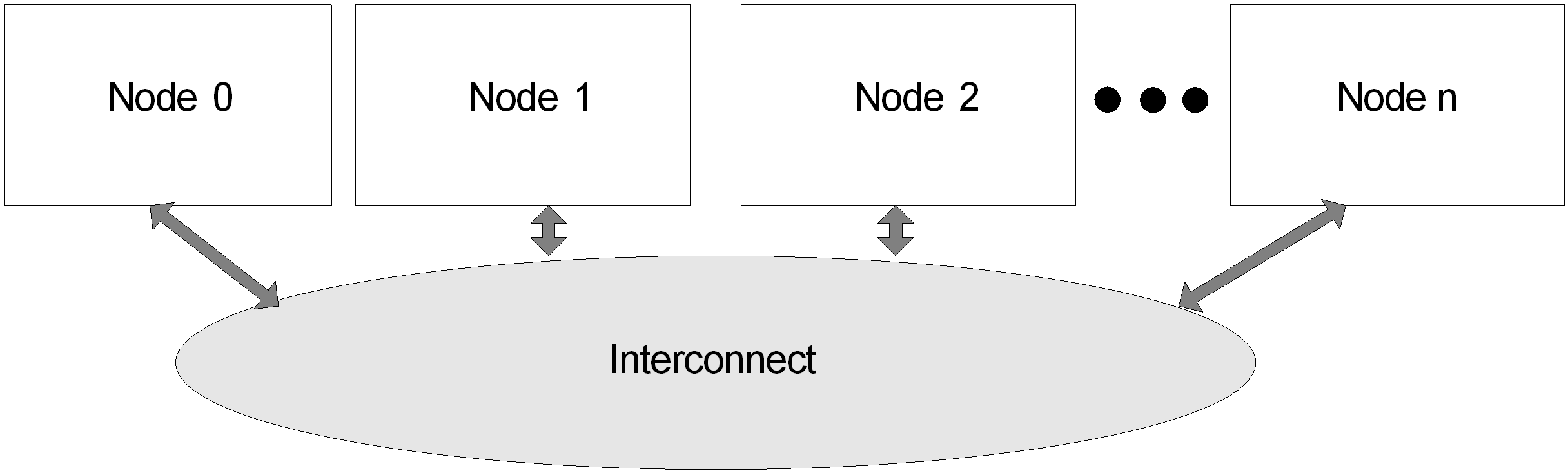
Fig. 6.5 System Locality information Table
The System Locality information Table diagrams a 4-node system where the nodes are numbered 0 through 3 (Node n = Node 3) and the granularity is at the node level for the NUMA distance information. In this example we assign System Localities / Proximity Domain numbers equal to the node numbers (0-3). The NUMA relative distances between proximity domains as implemented in this system are described in the matrix represented in Example Relative Distances Between Proximity Domains. Proximity Domains are represented by the numbers in the top row and left column. Distances are represented by the values in cells internal in the table from the domains.
ProximityDomain |
0 |
1 |
2 |
3 |
|---|---|---|---|---|
0 |
10 |
15 |
20 |
18 |
1 |
15 |
10 |
16 |
24 |
2 |
20 |
16 |
10 |
12 |
3 |
18 |
24 |
12 |
10 |
An example of these distances between proximity domains encoded in a System Locality Information Table for consumption by OSPM at boot time is described in the table below.
Field |
Byte Length |
Byte Offset |
Description |
|---|---|---|---|
Header |
|||
- Signature |
4 |
0 |
‘SLIT’. |
- Length |
4 |
4 |
60 |
- Revision |
1 |
8 |
1 |
- Checksum |
1 |
9 |
Entire table must sum to zero. |
- OEMID |
6 |
10 |
OEM ID. |
- OEM Table ID |
8 |
16 |
For the System Locality Information Table, the table ID is the manufacturer model ID. |
- OEM Revision |
4 |
24 |
OEM revision of System Locality Information Table for supplied OEM Table ID. |
- Creator ID |
4 |
28 |
Vendor ID of utility that created the table. For the DSDT, RSDT, SSDT, and PSDT tables, this is the ID for the ASL Compiler. |
|
4 |
32 |
Revision of utility that created the table. For the DSDT, RSDT, SSDT, and PSDT tables, this is the revision for the ASL Compiler. |
Number of System Localities |
8 |
36 |
4 |
Entry[0][0] |
1 |
44 |
10 |
Entry[0][1] |
1 |
45 |
15 |
Entry[0][2] |
1 |
46 |
20 |
Entry[0][3] |
1 |
47 |
18 |
Entry[1][0] |
1 |
48 |
15 |
Entry[1][1] |
1 |
49 |
10 |
Entry[1][2] |
1 |
50 |
16 |
Entry[1][3] |
1 |
51 |
24 |
Entry[2][0] |
1 |
52 |
20 |
Entry[2][1] |
1 |
53 |
16 |
Entry[2][2] |
1 |
54 |
10 |
Entry[2][3] |
1 |
55 |
12 |
Entry[3][0] |
1 |
56 |
18 |
Entry[3][1] |
1 |
57 |
24 |
Entry[3][2] |
1 |
58 |
12 |
Entry[3][3] |
1 |
59 |
10 |
If a new “Node 4” is added, then the following table represents the updated system’s NUMA relative distances of proximity domains.
Proximity Domain |
0 |
1 |
2 |
3 |
4 |
|---|---|---|---|---|---|
0 |
10 |
15 |
20 |
18 |
17 |
1 |
15 |
10 |
16 |
24 |
21 |
2 |
20 |
16 |
10 |
12 |
14 |
3 |
18 |
24 |
12 |
10 |
23 |
4 |
17 |
21 |
14 |
23 |
10 |
The new node’s _SLI object would evaluate to a buffer containing [17,21,14,23,10,17,21,14,23,10].
Note
Some systems support interleave memory across the nodes. The SLIT representation of these systems is implementation specific.
6.2.16. _SRS (Set Resource Settings)
This optional control method takes one byte stream argument that specifies a new resource allocation for a device. The resource descriptors in the byte stream argument must be specified exactly as listed in the _CRS byte stream - meaning that the identical resource descriptors must appear in the identical order, resulting in a buffer of exactly the same length. Optimizations such as changing an IRQ descriptor to an IRQNoFlags descriptor (or vice-versa) must not be performed. Similarly, changing StartDependentFn to StartDependentFnNoPri is not allowed. A _CRS object can be used as a template to ensure that the descriptors are in the correct format. For more information, see the _CRS object definition.
The settings must take effect before the _SRS control method returns.
This method must not reference any operation regions that have not been declared available by a _REG method.
If the device is disabled, _SRS enables the device at the specified resources. _SRS is not used to disable a device; use the _DIS control method instead.
Arguments: (1)
Arg0 - A Buffer containing a Resource Descriptor byte stream
Return Value:
None
6.2.17. _CCA (Cache Coherency Attribute)
The _CCA object returns whether or not a bus-master device supports hardware managed cache coherency. Expected values are 0 to indicate it is not supported, and 1 to indicate that it is supported. All other values are reserved.
On platforms for which existing default cache-coherency behavior of the OS is not adequate, _CCA enables the OS to adapt to the differences. If used, _CCA must be included under all bus-master-capable devices defined as children of \_SB, to ensure that the operating system knows when it can rely on hardware managed cache coherency. The value of _CCA is inherited by all descendants of these devices, so it need not be repeated for their children devices and will be ignored by OSPM if it is provided there. This includes slave devices on a shared DMA controller; thus these DMA controllers must also be defined in the namespace under the System Bus and include a _CCA object.
If a device indicates it does not have hardware cache coherency support, then OSPM must use a software cache flushing algorithm to ensure stale or invalid data is not accessed from the caches.
__CCA objects are only relevant for devices that can access CPU-visible memory, such as devices that are DMA capable. On ARM based systems, the _CCA object must be supplied all such devices. On Intel platforms, if the _CCA object is not supplied, the OSPM will assume the devices are hardware cache coherent.
Arguments:
None
Return Value:
An Integer indicating the device’s support for hardware cache coherency:
0 - The device does not have hardware managed cache coherency
1 - The device has hardware managed cache coherency
Other Values - Reserved
Note
There are restrictions related to when this object is evaluated which have implications for implementing this object as a control method. The _CCA method must only access Operation Regions that have been indicated to be available as defined by the _REG method. The _REG method is described in _REG (Region).
6.2.17.1. _CCA Example ASL:
Scope (\_SB) {
    ...
    Device (XHCI) {
        ...
        Name (_CCA, ZERO)     // Cache-incoherent bus-master, child of \\_SB
        ...
    }
    ...
    Device (PCI0) {           // Root PCI Bus
        ...
        Name (_CCA, ONE)      // Cache-coherent bus-master, child of \\_SB
        ...
        Device (PRT0) {
            ...               // Bus-master-capable, not a child of \\_SB
            ...               // Will inherit coherency from PCI0, no \_CCA required
            Device (NIC0) {
                ...           // Bus-master-capable, not a child of \\_SB
                ...           // Will inherit coherency from PRT0, no \_CCA required
            }
        }
    }
    ...
    Device (SDHC) {
        ...
        Name (_CCA, ONE)      // Cache-coherent bus-master-capable, child of \\_SB
        ...
    }
    ...
    Device (GPIO) {
        ...                   // Not bus-master-capable
        ...                   // \_CCA not valid
    }
    ...
    Device (DMAC) {
        ...                   // DMA controller; \_CCA must be specified
        Name (_CCA, ONE)      // Cache coherent bus-master, child of \\_SB
        ...
    }
    ...
    Device (SPI1) {
        ...
        Name (_CRS, ResourceTemplate()
            {
                FixedDMA(...) // Sharing the DMA, thus inherits coherency from it
                ...
                ...
            })
        ...                   // \_CCA not valid
      }
    }
6.2.18. _HMA(Heterogeneous Memory Attributes)
The Heterogeneous Memory Attributes Table (HMAT) defined in Heterogeneous Memory Attribute Table (HMAT) provides Heterogeneous Memory Attributes. Dynamic runtime reconfiguration of the system may cause proximities domains or memory attributes to change. If the “Reservation Hint” is set, new HMAT update shall not reset the “Reservation Hint” unless the memory range is removed.
_HMA is an optional object that enables the platform to provide the OS with updated Heterogeneous Memory Attributes information at runtime. _HMA provides OSPM with the latest HMAT in entirety overriding existing HMAT.
Arguments:
None
Return Value:
A Buffer containing entire HMAT.
Example ASL for _HMA usage:
Scope (\_SB) {
    Device (Dev1) {
    ...
    }
    Device (Dev2) {
    ...
    }
    Method (_HMA, 0) {
        Return (HMAD)
    }
}                         // end of \\_SB scope
6.3. Device Insertion, Removal, and Status Objects
The objects defined in this section provide mechanisms for handling dynamic insertion and removal of devices and for determining device and notification processing status.
Device insertion and removal objects are also used for docking and undocking mobile platforms to and from a peripheral expansion dock. These objects give information about whether or not devices are present, which devices are physically in the same device (independent of which bus the devices live on), and methods for controlling ejection or interlock mechanisms.
The system is more stable when removable devices have a software-controlled, VCR-style ejection mechanism instead of a “surprise-style” ejection mechanism. In this system, the eject button for a device does not immediately remove the device, but simply signals the operating system. OSPM then shuts down the device, closes open files, unloads the driver, and sends a command to the hardware to eject the device.
If the device is physically inserted while the system is in the working state (in other words, hot insertion), the hardware generates a general-purpose event.
The control method servicing the event uses the Notify(device,0) command to inform OSPM of the bus that the new device is on or the device object for the new device. If the Notify command points to the device object for the new device, the control method must have changed the device’s status returned by _STA to indicate that the device is now present. The performance of this process can be optimized by having the object of the Notify as close as possible, in the namespace hierarchy, to where the new device resides. The Notify command can also be used from the _WAK control method (see Section 7.4.5) to indicate device changes that may have occurred while the system was sleeping. For more information about the Notify command, see Section 5.6.6.
OSPM uses the identification and configuration objects to identify, configure, and load a device driver for the new device and any devices found below the device in the hierarchy.
If the device has a _LCK control method, OSPM may later run this control method to lock the device.
The new device referred to in step 2 need not be a single device, but could be a whole tree of devices. For example, it could point to the PCI-PCI bridge docking connector. OSPM will then load and configure all devices it found below that bridge. The control method can also point to several different devices in the hierarchy if the new devices do not all live under the same bus. (in other words, more than one bus goes through the connector).
For removing devices, ACPI supports both hot removal (system is in the S0 state), and warm removal (system is in a sleep state: S1-S4). This is done using the _EJx control methods. Devices that can be ejected include an _EJx control method for each sleeping state the device supports (a maximum of 2 _EJx objects can be listed). For example, hot removal devices would supply an _EJ0; warm removal devices would use one of _EJ1-EJ4. These control methods are used to signal the hardware when an eject is to occur.
The sequence of events for dynamically removing a device goes as follows:
The eject button is pressed and generates a general-purpose event. (If the system was in a sleeping state, it should wake the system).
The control method for the event uses the Notify(device, 3) command to inform OSPM which specific device the user has requested to eject. Notify does not need to be called for every device that may be ejected, but for the top-level device. Any child devices in the hierarchy or any ejection-dependent devices on this device (as described by _EJD, below) are automatically removed.
The OS shuts down and unloads devices that will be removed.
If the device has a _LCK control method, OSPM runs this control method to unlock the device.
The OS looks to see what _EJx control methods are present for the device. If the removal event will cause the system to switch to battery power (in other words, an undock) and the battery is low, dead, or not present, OSPM uses the lowest supported sleep state _EJx listed; otherwise it uses the highest state _EJx. Having made this decision, OSPM runs the appropriate _EJx control method to prepare the hardware for eject.
Warm removal requires that the system be put in a sleep state. If the removal will be a warm removal, OSPM puts the system in the appropriate Sx state. If the removal will be a hot removal, OSPM skips to step 8, below.
For warm removal, the system is put in a sleep state. Hardware then uses any motors, and so on, to eject the device. Immediately after ejection, the hardware transitions the system to S0. If the system was sleeping when the eject notification came in, the OS returns the system to a sleeping state consistent with the user’s wake settings.
OSPM calls _STA to determine if the eject successfully occurred. (In this case, control methods do not need to use the Notify(device,3) command to tell OSPM of the change in _STA) If there were any mechanical failures, _STA returns 3: device present and not functioning, and OSPM informs the user of the problem.
Note
This mechanism is the same for removing a single device and for removing several devices, as in an undock.
ACPI does not disallow surprise-style removal of devices; however, this type of removal is not recommended because system and data integrity cannot be guaranteed when a surprise-style removal occurs. Because the OS is not informed, its device drivers cannot save data buffers and it cannot stop accesses to the device before the device is removed. To handle surprise-style removal, a general-purpose event must be raised. Its associated control method must use the Notify command to indicate which bus the device was removed from.
The device insertion and removal objects are listed in the table below.
Object |
Description |
|---|---|
_EDL |
Object that evaluates to a package of namespace references of device objects that depend on the device containing _EDL. |
_EJD |
Object that evaluates to the name of a device object on which a device depends. Whenever the named device is ejected, the dependent device must receive an ejection notification. |
_EJx |
Control method that ejects a device. |
_LCK |
Control method that locks or unlocks a device. |
_OST |
Control method invoked by OSPM to convey processing status to the platform. |
_RMV |
Object that indicates that the given device is removable. |
_STA |
Control method that returns a device’s status. |
6.3.1. _EDL (Eject Device List)
This object evaluates to a package of namespace references containing the names of device objects that depend on the device under which the _EDL object is declared. This is primarily used to support docking stations. Before the device under which the _EDL object is declared may be ejected, OSPM prepares the devices listed in the _EDL object for physical removal.
Arguments:
None
Return Value:
A variable-length Package containing a list of namespace references
Before OSPM ejects a device via the device’s _EJx methods, all dependent devices listed in the package returned by _EDL are prepared for removal. Notice that _EJx methods under the dependent devices are not executed.
When describing a platform that includes a docking station, an _EDL object is declared under the docking station device. For example, if a mobile system can attach to two different types of docking stations, _EDL is declared under both docking station devices and evaluates to the packaged list of devices that must be ejected when the system is ejected from the docking station.
An ACPI-compliant OS evaluates the _EDL method just prior to ejecting the device.
6.3.2. _EJD (Ejection Dependent Device)
This object is used to specify the name of a device on which the device, under which this object is declared, is dependent. This object is primarily used to support docking stations. Before the device indicated by _EJD is ejected, OSPM will prepare the dependent device (in other words, the device under which this object is declared) for removal.
Arguments:
None
Return Value:
A String containing the device name
_EJD is evaluated once when the ACPI table loads. The EJx methods of the device indicated by _EJD will be used to eject all the dependent devices. A device’s dependents will be ejected when the device itself is ejected.
Note
OSPM will not execute a dependent device’s _EJx methods when the device indicated by _EJD is ejected.
When describing a platform that includes a docking station, usually more than one _EJD object will be needed. For example, if a dock attaches both a PCI device and an ACPI-configured device to a mobile system, then both the PCI device description package and the ACPI-configured device description package must include an _EJD object that evaluates to the name of the docking station (the name specified in an _ADR or _HID object in the docking station’s description package). Thus, when the docking connector signals an eject request, OSPM first attempts to disable and unload the drivers for both the PCI and ACPI configured devices.
Note
An ACPI 1.0 OS evaluates the _EJD methods only once during the table load process. This greatly restricts a table designer’s freedom to describe dynamic dependencies such as those created in scenarios with multiple docking stations. This restriction is illustrated in the example below; the _EJD information supplied via and ACPI 1.0-compatible namespace omits the IDE2 device from DOCK2’s list of ejection dependencies. Starting in ACPI 2.0, OSPM is presented with a more in-depth view of the ejection dependencies in a system by use of the _EDL methods.
Example
An example use of _EJD and _EDL is as follows:
Scope(\_SB.PCI0) {
   Device(DOCK1) {             // Pass through dock - DOCK1
      Name(_ADR, ...)
      Method(_EJ0, 0) {...}
      Method(_DCK, 1) {...}
      Name(_BDN, ...)
      Method(_STA, 0) {0xF}
      Name(_EDL, Package( ) {  // DOCK1 has two dependent devices - IDE2 and CB2
      \\_SB.PCI0.IDE2,
      \\_SB.PCI0.CB2})
   }
   Device(DOCK2) {             // Pass through dock - DOCK2
      Name(_ADR, ...)
      Method(_EJ0, 0) {...}
      Method(_DCK, 1) {...}
      Name(_BDN, ...)
      Method(_STA, 0) {0x0}
      Name(_EDL, Package( ) {  // DOCK2 has one dependent device - IDE2
      \\_SB.PCI0.IDE2})
   }
   Device(IDE1) {              // IDE Drive1 not dependent on the dock
      Name(_ADR, ...)
   }
   Device(IDE2) {              // IDE Drive2
      Name(_ADR, ...)
      Name(_EJD,"\\_SB.PCI0.DOCK1")                // Dependent on DOCK1
   }
   Device(CB2) {               // CardBus Controller
      Name(_ADR, ...)
      Name(_EJD,"\\_SB.PCI0.DOCK1")                // Dependent on DOCK1
   }
}                              // end \\_SB.PCIO
6.3.3. _EJx (Eject)
These control methods are optional and are supplied for devices that support a software-controlled VCR-style ejection mechanism or that require an action be performed such as isolation of power/data lines before the device can be removed from the system. To support warm (system is in a sleep state) and hot (system is in S0) removal, an _EJx control method is listed for each sleep state from which the device supports removal, where x is the sleeping state supported. For example, _EJ0 indicates the device supports hot removal; _EJ1-EJ4 indicate the device supports warm removal.
Arguments: (1)
Arg0 - An Integer containing a device ejection control
0 - Cancel a mark for ejection request (EJ0 will never be called with this value)
1 - Hot eject or mark for ejection
Return Value:
None
For hot removal, the device must be immediately ejected when OSPM calls the _EJ0 control method. The _EJ0 control method does not return until ejection is complete. After calling _EJ0, OSPM verifies the device no longer exists to determine if the eject succeeded. For _HID devices, OSPM evaluates the _STA method. For _ADR devices, OSPM checks with the bus driver for that device.
For warm removal, the _EJ1-_EJ4 control methods do not cause the device to be immediately ejected. Instead, they set proprietary registers to prepare the hardware to eject when the system goes into the given sleep state. The hardware ejects the device only after OSPM has put the system in a sleep state by writing to the SLP_EN register. After the system resumes, OSPM calls _STA to determine if the eject succeeded.
A device object may have multiple _EJx control methods. First, it lists an EJx control method for the preferred sleeping state to eject the device. Optionally, the device may list an EJ4 control method to be used when the system has no power (for example, no battery) after the eject. For example, a hot-docking notebook might list _EJ0 and _EJ4.
6.3.4. _LCK (Lock)
This control method is optional and is required only for a device that supports a software-controlled locking mechanism. When the OS invokes this control method, the associated device is to be locked or unlocked based upon the value of the argument that is passed. On a lock request, the control method must not complete until the device is completely locked.
Arguments:
Arg0 - An Integer containing a device lock control
0 - Unlock the device
1 - Lock the device
Return Value:
None
When describing a platform, devices use either a _LCK control method or an _EJx control method for a device.
6.3.5. _OST (OSPM Status Indication)
This object is an optional control method that is invoked by OSPM to indicate processing status to the platform. During device ejection, device hot add, Error Disconnect Recover, or other event processing, OSPM may need to perform specific handshaking with the platform. OSPM may also need to indicate to the platform its inability to complete a requested operation; for example, when a user presses an ejection button for a device that is currently in use or is otherwise currently incapable of being ejected. In this case, the processing of the ACPI Eject Request notification by OSPM fails. OSPM may indicate this failure to the platform through the invocation of the _OST control method. As a result of the status notification indicating ejection failure, the platform may take certain action including reissuing the notification or perhaps turning on an appropriate indicator light to signal the failure to the user.
Arguments: (3)
Arg0 - An Integer containing the source event
Arg1 - An Integer containing the status code
Arg2 - A Buffer containing status information
Return Value:
None
Argument Information:
Arg0 - source_event: DWordConst
If the value of source_event is <= 0xFF, this argument is the ACPI notification value whose processing generated the status indication. This is the value that was passed into the Notify operator.
If the value of source_event is 0x100 or greater then the OSPM status indication is a result of an OSPM action as indicated in OST Source Event Codes. For example, a value of 0x103 will be passed into _OST for this argument upon the failure of a user interface invoked device ejection.
If OSPM is unable to identify the originating notification value, OSPM invokes _OST with a value that contains all bits set (ones) for this parameter.
Arg1 – Status Code: DWordConst. OSPM indicates a notification value specific status. See Table 6.22, Table 6.23, and Table 6.25 for status code descriptions.
Arg2 - A buffer containing detailed OSPM-specific information about the status indication. This argument may be null.
Source Event Code |
Description |
|---|---|
0-0xFF |
Reserved for Notification Values |
0x100 |
Operation System Shutdown Processing |
0x101-0x102 |
Reserved |
0x103 |
Ejection Processing |
0x104-0x1FF |
Reserved |
0x200 |
Insertion Processing |
0x201-0xFFFFFFFF |
Reserved |
Status Code |
Description |
|---|---|
0 |
Success |
1 |
Non-specific failure |
2 |
Unrecognized Notify Code |
3-0x7F |
Reserved |
0x80-0xFFFFFFFF |
Notification value specific status codes |
Status Code |
Description |
|---|---|
0x80 |
OS Shutdown Request denied |
0x81 |
OS Shutdown in progress |
0x82 |
OS Shutdown completed |
0x83 |
OS Graceful Shutdown not supported |
0x84-0xFFFFFFFF |
Reserved |
6.3.5.1. Processing Sequence for Graceful Shutdown Request:
Following receipt of the Graceful Shutdown Request (see Table 5.155, value 0x81), the OS will be responsible for responding with one of the following status codes:
0x80 (OS Shutdown Request denied) - This value will be sent if the OS is not capable of performing a graceful shutdown.
0x81 (OS Shutdown in progress) - The OS has initiated the graceful shutdown procedure.
0x83 (OS Graceful Shutdown not supported) - The OS does not support the Graceful Shutdown Request.
If the OS does initiate a graceful shutdown it should continue to generate the “OS Shutdown in progress” message (_OST source event 0x100 status code 0x81) every 10 seconds. This functions as a heartbeat so that the service which requested the graceful shutdown knows that the request is currently being processed. The platform should assume that the OS shutdown is not proceeding if it does not receive the “OS Shutdown in progress” message for 60 seconds.
When the graceful shutdown procedure has completed the OSPM will send the “OS Shutdown completed” message and then transition the platform to the G2 “soft-off” power state.
Status Code |
Description |
|---|---|
0x80 |
Device ejection not supported by OSPM |
0x81 |
Device in use by application |
0x82 |
Device Busy |
0x83 |
Ejection dependency is busy or not supported for ejection by OSPM |
0x84 |
Ejection is in progress (pending) |
0x85-0xFFFFFFFF |
Reserved |
Status Code |
Description |
|---|---|
0x80 |
Device insertion in progress (pending) |
0x81 |
Device driver load failure |
0x82 |
Device insertion not supported by OSPM |
0x83-0x8F |
Reserved |
0x90-0x9F |
Insertion failure - Resources Unavailable as described by the following bit encodings: Bit [3] Bus or Segment Numbers Bit [2] Interrupts Bit [1] I/O Bit [0] Memory |
0xA0-0xFFFFFFFF |
Reserved |
It is possible for the platform to issue multiple notifications to OSPM and for OSPM to process the notifications asynchronously. As such, OSPM may invoke _OST for notifications independent of the order the notification are conveyed by the platform or by software to OSPM.
The figure below provides and example event flow of device ejection on a platform employing the _OST object.
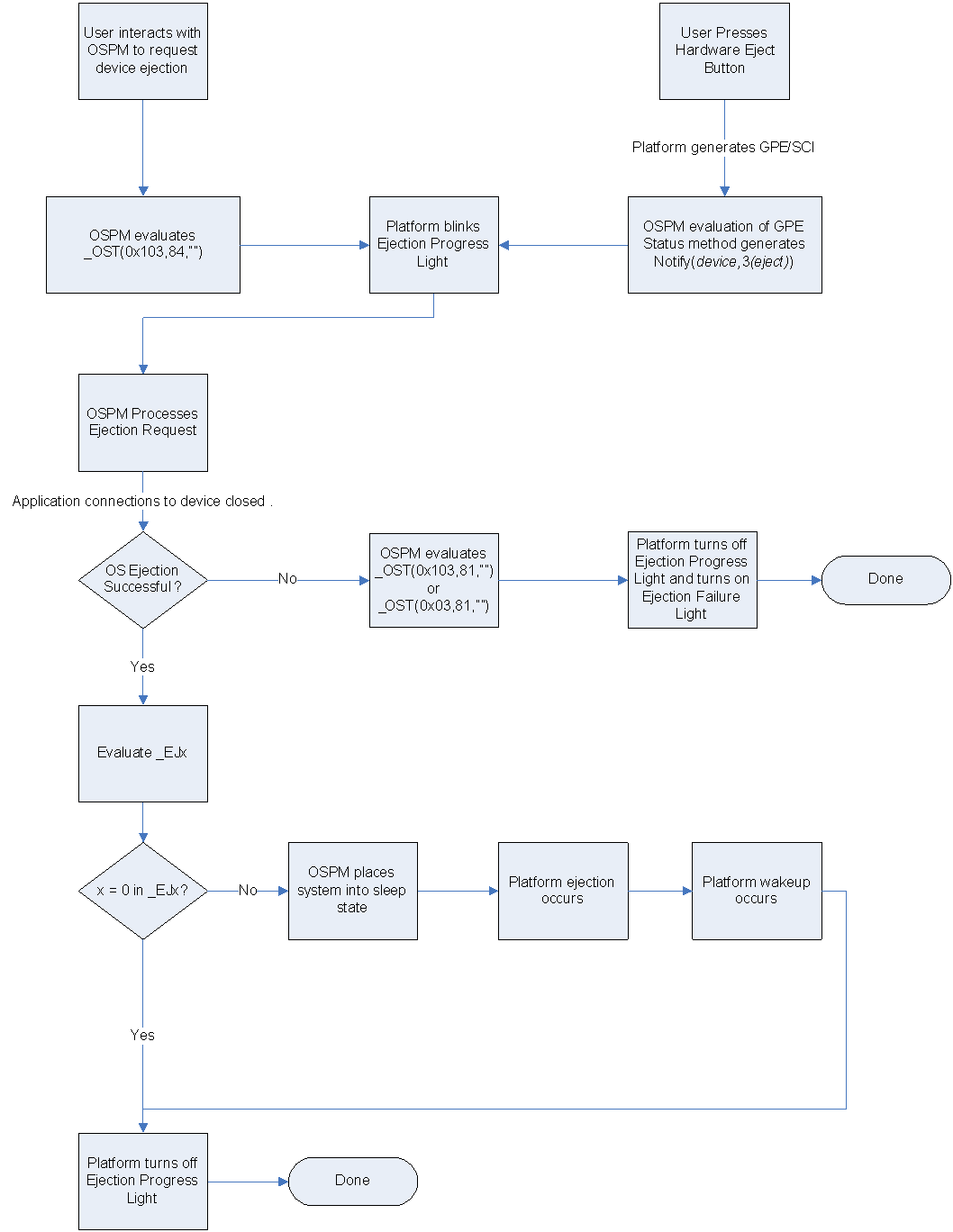
Fig. 6.6 Device Ejection Flow Example Using _OST
Note
To maintain compatibility with OSPM implementations of previous revisions of the ACPI specification, the platform must not rely on OSPM’s evaluation of the _OST object for proper platform operation.
Example ASL for _OST usage:
External (\_SB.PCI4, DeviceObj)
Scope(\_SB.PCI4) {
   OperationRegion(LED1, SystemIO, 0x10C0, 0x20)
   Field(LED1, AnyAcc, NoLock, Preserve)
   {                              // LED controls
      S0LE, 1,                    // Slot 0 Ejection Progress LED
      S0LF, 1,                    // Slot 0 Ejection Failure LED
      S1LE, 1,                    // Slot 1 Ejection Progress LED
      S1LF, 1,                    // Slot 1 Ejection Failure LED
      S2LE, 1,                    // Slot 2 Ejection Progress LED
      S2LF, 1,                    // Slot 2 Ejection Failure LED
      S3LE, 1,                    // Slot 3 Ejection Progress LED
      S3LF, 1                     // Slot 3 Ejection Failure LED
   }
   Device(SLT3) { // hot plug device
      Name(_ADR, 0x000C0003)
      Method(_OST, 3, Serialized) { // OS calls \_OST with notify code 3 or 0x103
                                    // and status codes 0x80-0x83
                                    // to indicate a hot remove request failure.
                                    // to indicate a hot remove request failure.
                                    // Status code 0x84 indicates an ejection
                                    // request pending.
         If(LEqual(Arg0,Ones))      // Unspecified event
         {
                                    // Perform generic event processing here
         }
         Switch(And(Arg0,0xFF))     // Mask to retain low byte
         {
            Case(0x03)              // Ejection request
            {
               Switch(Arg1)
               {
                  Case(Package(){0x80, 0x81, 0x82, 0x83})
                  {                 // Ejection Failure for some reason
                     Store(Zero, ^^S3LE)    // Turn off Ejection Progress LED
                     Store(One, ^^S3LF)     // Turn on Ejection Failure LED
                  }
                  Case(0x84)        // Eject request pending
                  {
                     Store(One, ^^S3LE)     // Turn on Ejection Request LED
                     Store(Zero, ^^S3LF)    // Turn off Ejection Failure LED
                  }
               }
            }
         }
      }                             // end \_OST
      Method(_EJ0, 1)               // Successful ejection sequence
      {
         Store(Zero, ^^S3LE)        // Turn off Ejection Progress LED
      }
   }                                // end SLT3
}                                   // end scope \\_SB.PCI4
Scope (\_GPE)
{
   Method(_E13)
   {
      Store(One, \\_SB.PCI4.S3LE)   // Turn on ejection request LED
      Notify(\_SB.PCI4.SLT3, 3)     // Ejection request driven from GPE13
   }
}
6.3.5.2. Processing Sequence for Error Disconnect Recover
If the OS attempts recovery operation following the receipt of the Error Disconnect Recover Request (see IPMI Status Codes , value 0x0F) the OS will be responsible for invoking _OST with one of the following status codes in the lower word of Arg1:
0x80 (Success) -This value will be sent if the OS successfully recovers all the child devices affected by Error Disconnect Recover, reconfigures then and brings them back to functional state. All child devices are accessible at the time _OST is evaluated.
0x81 (Not recovered) - The OS did not successfully recover one or more child devices that were affected by Error Disconnect Recover. Access to the child devices affected by Error Disconnect Recover may be unreliable.
The upper word of Arg1 can be used to communicate bus-specific status information.
6.3.6. _RMV (Remove)
The optional _RMV object indicates to OSPM whether the device can be removed while the system is in the working state and does not require any ACPI system firmware actions to be performed for the device to be safely removed from the system (in other words, any device that only supports surprise-style removal). Any such removable device that does not have _LCK or _EJx control methods must have an _RMV object. This allows OSPM to indicate to the user that the device can be removed and to provide a way for shutting down the device before removing it. OSPM will transition the device into D3 before telling the user it is safe to remove the device.
This method is reevaluated after a device-check notification.
Arguments:
None
Return Value:
An Integer containing the device removal status:
0 - The device cannot be removed
1 - The device can be removed
Note
Operating Systems implementing ACPI 1.0 interpret the presence of this object to mean that the device is removable.
6.3.7. _STA (Device Status)
This object returns the current status of a device, which can be one of the following: enabled, disabled, or removed.
OSPM evaluates the _STA object before it evaluates a device _INI method. The return values of the Present and Functioning bits determines whether _INI should be evaluated and whether children of the device should be enumerated and initialized. See _INI (Init) .
If a device object describes a device that is not on an enumerable bus and the device object does not have an _STA object, then OSPM assumes that the device is present, enabled, shown in the UI, and functioning.
This method must not reference any operation regions that have not been declared available by a _REG method.
Arguments:
None
Return Value:
An Integer containing a device status bitmap:
Bit [0] - Set if the device is present.
Bit [1] - Set if the device is enabled and decoding its resources.
Bit [2] - Set if the device should be shown in the UI.
Bit [3] - Set if the device is functioning properly (cleared if device failed its diagnostics).
Bit [4] - Set if the battery is present.
Bits [31:5] - Reserved (must be cleared).
Return Value Information
If bit [0] is cleared, then bit 1 must also be cleared (in other words, a device that is not present cannot be enabled).
A device can only decode its hardware resources if both bits 0 and 1 are set. If the device is not present (bit [0] cleared) or not enabled (bit [1] cleared), then the device must not decode its resources.
If a device is present in the machine, but should not be displayed in OSPM user interface, bit 2 is cleared. For example, a notebook could have joystick hardware (thus it is present and decoding its resources), but the connector for plugging in the joystick requires a port replicator. If the port replicator is not plugged in, the joystick should not appear in the UI, so bit [2] is cleared.
_STA may return bit 0 clear (not present) with bit [3] set (device is functional). This case is used to indicate a valid device for which no device driver should be loaded (for example, a bridge device.) Children of this device may be present and valid. OSPM should continue enumeration below a device whose _STA returns this bit combination.
Bit [4] of _STA applies only to the Control Method Battery Device (PNP0C0A). For all other devices, OSPM must ignore this bit.
If a device object (including the processor object) does not have an _STA object, then OSPM assumes that all of the above bits are set (i.e., the device is present, enabled, shown in the UI, and functioning).
6.4. Resource Data Types for ACPI
The _CRS, _PRS, and _SRS control methods use packages of resource descriptors to describe the resource requirements of devices.
6.4.1. ASL Macros for Resource Descriptors
ASL includes some macros for creating resource descriptors. The ASL syntax for these macros is defined in ASL Operator Reference, along with the other ASL operators.
6.4.2. Small Resource Data Type
A small resource data type may be 2 to 8 bytes in size and adheres to the following format:
Offset |
Field Description |
|---|---|
Byte 0 |
Tag Bit [7]: Type-0 (Small item) || Tag Bits [6:3]: Small item name || Tag Bits [2:0]: Length- n bytes |
Bytes 1 to n |
Data bytes (Length 0 - 7) |
The following small information items are currently defined for Plug and Play devices:
Small Item Name |
Value |
|---|---|
Reserved |
0x00-0x03 |
IRQ Format Descriptor |
0x04 |
DMA Format Descriptor |
0x05 |
Start Dependent Functions Descriptor |
0x06 |
End Dependent Functions Descriptor |
0x07 |
I/O Port Descriptor |
0x08 |
Fixed Location I/O Port Descriptor |
0x09 |
Fixed DMA Descriptor |
0x0A |
Reserved |
0x0B-0x0D |
Vendor Defined Descriptor |
0x0E |
End Tag Descriptor |
0x0F |
6.4.2.1. IRQ Descriptor
Type 0, Small Item Name 0x4, Length = 2 or 3
The IRQ data structure indicates that the device uses an interrupt level and supplies a mask with bits set indicating the levels implemented in this device. For standard PC-AT implementation there are 15 possible interrupts so a two-byte field is used. This structure is repeated for each separate interrupt required.
Offset |
Field Name |
|---|---|
Byte 0 |
Value = 0x22 or 0x23 (0010001nB) - Type = 0, Small item name = 0x4, Length = 2 or 3 |
Byte 1 |
IRQ mask bits[7:0], _INT Bit [0] represents IRQ0, bit[1] is IRQ1, and so on. |
Byte 2 |
IRQ mask bits[15:8], _INT Bit [0] represents IRQ8, bit[1] is IRQ9, and so on. |
Byte 3 |
IRQ Information. Each bit, when set, indicates this device is capable of driving a certain type of interrupt. (Optional–if not included then assume edge sensitive, high true interrupts.) These bits can be used both for reporting and setting IRQ resources. Note: This descriptor is meant for describing interrupts that are connected to PIC-compatible interrupt controllers, which can only be programmed for Active-High-Edge-Triggered or Active-Low-Level-Triggered interrupts. Any other combination is invalid. The Extended Interrupt Descriptor can be used to describe other combinations:
Bit [7:6] Reserved (must be 0)
Bit [5] Wake Capability, _WKC
0x0 = Not Wake Capable: This interrupt is not capable of waking the system.
0x1 = Wake Capable: This interrupt is capable of waking the system from a low-power idle state or a system sleep state.
Bit [4] Interrupt Sharing, _SHR
0x0 = Exclusive: This interrupt is not shared with other devices.
0x1 = Shared: This interrupt is shared with other devices.
Bit [3] Interrupt Polarity, _LL
0 Active-High - This interrupt is sampled when the signal is high, or true
1 Active-Low - This interrupt is sampled when the signal is low, or false.
Bit [2:1] Ignored
Bit [0] Interrupt Mode, _HE
0 Level-Triggered - Interrupt is triggered in response to signal in a low state.
1 Edge-Triggered - Interrupt is triggered in response to a change in signal state from low to high.
|
Note
Low true, level sensitive interrupts may be electrically shared, but the process of how this might work is beyond the scope of this specification.
Note
If byte 3 is not included, High true, edge sensitive, non-shareable is assumed.
See IRQ (Interrupt Resource Descriptor Macro) for a description of the ASL macros that create an IRQ descriptor.
6.4.2.2. DMA Descriptor
Type 0, Small Item Name 0x5, Length = 2
The DMA data structure indicates that the device uses a DMA channel and supplies a mask with bits set indicating the channels actually implemented in this device. This structure is repeated for each separate channel required.
Offset |
Field Name |
|---|---|
Byte 0 |
Value = 0x2A (00101010B) - Type = 0, Small item name = 0x5, Length = 2 |
Byte 1 |
DMA channel mask bits [7:0] (channels 0 - 7), _DMA - Bit [0] is channel 0, etc. |
Byte 2 |
Bit [7] Reserved (must be 0)
Bits [6:5] DMA channel speed supported, _TYP:
00 Indicates compatibility mode
01 Indicates Type A DMA as described in the EISA
10 Indicates Type B DMA
11 Indicates Type F
Bits [4:3] Ignored
Bit [2] Logical device bus master status, _BM:
0 Logical device is not a bus master
1 Logical device is a bus master
Bits [1:0] DMA transfer type preference, _SIZ:
00 8-bit only
01 8- and 16-bit
10 16-bit only
11 Reserved
|
See DMA (DMA Resource Descriptor Macro) for a description of the ASL macro that creates a DMA descriptor.
6.4.2.3. Start Dependent Functions Descriptor
Type 0, Small Item Name 0x6, Length = 0 or 1
Each logical device requires a set of resources. This set of resources may have interdependencies that need to be expressed to allow arbitration software to make resource allocation decisions about the logical device. Dependent functions are used to express these interdependencies. The data structure definitions for dependent functions are shown here. For a detailed description of the use of dependent functions refer to the next section.
Offset |
Field Name |
|---|---|
Byte 0 |
Value = 0x30 or 0x31 (0011000nB)
Type = 0, small item name = 0x6
Length = 0 or 1
|
Start Dependent Function fields may be of length 0 or 1 bytes. The extra byte is optionally used to denote the compatibility or performance/robustness priority for the resource group following the Start DF tag. The compatibility priority is a ranking of configurations for compatibility with legacy operating systems. This is the same as the priority used in the PNPBIOS interface. For example, for compatibility reasons, the preferred configuration for COM1 is IRQ4, I/O 3F8-3FF. The performance/robustness performance is a ranking of configurations for performance and robustness reasons. For example, a device may have a high-performance, bus mastering configuration that may not be supported by legacy operating systems. The bus-mastering configuration would have the highest performance/robustness priority while its polled I/O mode might have the highest compatibility priority.
If the Priority byte is not included, this indicates the dependent function priority is ‘acceptable’. This byte is defined as:
Bits |
Definition |
|---|---|
1:0 |
Compatibility priority. Acceptable values are:
0 Good configuration: Highest Priority and preferred configuration
1 Acceptable configuration: Lower Priority but acceptable configuration
2 Sub-optimal configuration: Functional configuration but not optimal
3 Reserved
|
3:2 |
Performance/robustness. Acceptable values are:
0 Good configuration: Highest Priority and preferred configuration
1 Acceptable configuration: Lower Priority but acceptable configuration
2 Sub-optimal configuration: Functional configuration but not optimal
3 Reserved
|
7:4 |
Reserved (must be 0) |
Notice that if multiple Dependent Functions have the same priority, they are further prioritized by the order in which they appear in the resource data structure. The Dependent Function that appears earliest (nearest the beginning) in the structure has the highest priority, and so on.
See StartDependentFn (Start Dependent Function Resource Descriptor Macro) for a description of the ASL macro that creates a Start Dependent Function descriptor.
6.4.2.4. End Dependent Functions Descriptor
Type 0, Small Item Name 0x7, Length = 0
Only one End Dependent Function item is allowed per logical device. This enforces the fact that Dependent Functions cannot be nested.
Offset |
Field Name |
Byte 0 |
Value = 0x38 (00111000B) - Type = 0, Small item name = 0x7, Length =0 |
See EndDependentFn (End Dependent Function Resource Descriptor Macro) for a description of the ASL macro that creates an End Dependent Functions descriptor.
6.4.2.5. I/O Port Descriptor
Type 0, Small Item Name 0x8, Length = 7
There are two types of descriptors for I/O ranges. The first descriptor is a full function descriptor for programmable devices. The second descriptor is a minimal descriptor for old ISA cards with fixed I/O requirements that use a 10-bit ISA address decode. The first type descriptor can also be used to describe fixed I/O requirements for ISA cards that require a 16-bit address decode. This is accomplished by setting the range minimum base address and range maximum base address to the same fixed I/O value.
Offset |
Field Name |
Definition |
|---|---|---|
Byte 0 |
I/O Port Descriptor |
Value = 0x47 (01000111B) - Type = 0, Small item name = 0x8, Length = 7 |
Byte 1 |
Information |
Bits [7:1] Reserved and must be 0 Bit [0] (_DEC) 1 The logical device decodes 16-bit addresses 0 The logical device only decodes address bits[9:0] |
Byte 2 |
Range minimum base address, _MIN bits[7:0] |
Address bits [7:0] of the minimum base I/O address that the card may be configured for. |
Byte 3 |
Range minimum base address, _MIN bits[15:8] |
Address bits [15:8] of the minimum base I/O address that the card may be configured for. |
Byte 4 |
Range maximum base address, _MAX bits[7:0] |
Address bits [7:0] of the maximum base I/O address that the card may be configured for. |
Byte 5 |
Range maximum base address, _MAX bits[15:8] |
Address bits [15:8] of the maximum base I/O address that the card may be configured for. |
Byte 6 |
Base alignment, _ALN |
Alignment for minimum base address, increment in 1-byte blocks. |
Byte 7 |
Range length, _LEN |
The number of contiguous I/O ports requested. |
See IO (IO Resource Descriptor Macro) for a description of the ASL macro that creates an I/O Port descriptor.
6.4.2.6. Fixed Location I/O Port Descriptor
Type 0, Small Item Name 0x9, Length = 3
This descriptor is used to describe 10-bit I/O locations.
Offset |
Field Name |
Definition |
|---|---|---|
Byte 0 |
Fixed Location I/O Port Descriptor |
Value = 0x4B (01001011B) - Type = 0, Small item name = 0x9, Length = 3 |
Byte 1 |
Range base address, _BAS bits[7:0] |
Address bits [7:0] of the base I/O address that the card may be configured for. This descriptor assumes a 10-bit ISA address decode. |
Byte 2 |
Range base address, _BAS bits[9:8] |
Address bits [9:8] of the base I/O address that the card may be configured for. This descriptor assumes a 10-bit ISA address decode. |
Byte 3 |
Range length, _LEN |
The number of contiguous I/O ports requested. |
See FixedIO (Fixed IO Resource Descriptor Macro) for a description of the ASL macro that creates a Fixed I/O Port descriptor.
6.4.2.7. Fixed DMA Descriptor
Type 0, Small Item Name 0xA, Length = 5
The Fixed DMA descriptor provides a means for platforms to statically assign DMA request lines and channels to devices connected to a shared DMA controller. This descriptor differs from the DMA descriptor in that it supports many more DMA request lines and DMA controller channels, as well as a flexible mapping between the two. The width of the bus used for transfers to the device is also provided. This structure is repeated for each separate request line/channel pair required, and can only be used in the _CRS object. (Dynamic arbitration of Fixed DMA resource is not supported.)
Offset |
Field Name |
|---|---|
Byte 0 |
Value = 0x55 (01010101B) - Type = 0, Small item name = 0xA, Length = 0x5 |
Byte 1 |
DMA Request Line bits [7:0] _DMA[7:0]. A platform-relative number uniquely identifying the request line assigned. Request line-to-Controller mapping is done in a controller-specific OS driver. |
Byte 2 |
DMA Request Line bits [15:8] _DMA[15:8] |
Byte 3 |
DMA Channel bits[7:0] _TYP[7:0]. A controller-relative number uniquely identifying the controller’s logical channel assigned. Channel numbers can be shared by multiple request lines. |
Byte 4 |
DMA Channel bits[15:8] _TYP[15:8] |
Byte 5 |
DMA Transfer Width. _SIZ. Bus width that the device connected to this request line supports. 0x00 8-bit 0x01 16-bit 0x02 32-bit 0x03 64-bit 0x04 128-bit 0x05 256-bit 0x06-0xFF Reserved |
6.4.2.8. Vendor-Defined Descriptor, Type 0
Type 0, Small Item Name 0xE, Length = 1 to 7
The vendor defined resource data type is for vendor use.
Offset |
Field Name |
|---|---|
Byte 0 |
Value = 0x71 - 0x77 (01110nnnB) - Type = 0, small item name = 0xE, Length = 1-7 |
Byte 1 to 7 |
Vendor defined |
See VendorShort (Short Vendor Resource Descriptor) for a description of the ASL macro that creates a short vendor-defined resource descriptor.
6.4.2.9. End Tag
Type 0, Small Item Name 0xF, Length = 1
The End tag identifies an end of resource data.
Note
If the checksum field is zero, the resource data is treated as if the checksum operation succeeded. Configuration proceeds normally.
Offset |
Field Name |
|---|---|
Byte 0 |
Value = 0x79 (01111001B) - Type = 0, Small item name = 0xF, Length = 1 |
Byte 1 |
Checksum covering all resource data after the serial identifier. This checksum is generated such that adding it to the sum of all the data bytes will produce a zero sum. |
The End Tag is automatically generated by the ASL compiler at the end of the ResourceTemplate statement.
6.4.3. Large Resource Data Type
To allow for larger amounts of data to be included in the configuration data structure the large format is shown below. This includes a 16-bit length field allowing up to 64 KB of data.
Offset |
Field Name |
Byte 0 |
Value = 1xxxxxxxB
Type = 1 (Large item)
Large item name = xxxxxxxB
|
Byte 1 |
Length of data items bits[7:0] |
Byte 2 |
Length of data items bits[15:8] |
Bytes 3 to (Length + 2) |
Actual data items |
The following large information items are currently defined:
Large Item Name |
Value |
|---|---|
Reserved |
0x00 |
24-Bit Memory Range Descriptor |
0x01 |
Generic Register Descriptor |
0x02 |
Reserved |
0x03 |
Vendor-Defined Descriptor |
0x04 |
32-Bit Memory Range Descriptor |
0x05 |
32-Bit Fixed Memory Range Descriptor |
0x06 |
Address Space Resource Descriptors |
0x07 |
Word Address Space Descriptor |
0x08 |
Extended Interrupt Descriptor |
0x09 |
QWord Address Space Descriptor |
0x0A |
Extended Address Space Descriptor |
0x0B |
GPIO Connection Descriptor |
0x0C |
Pin Function Descriptor |
0x0D |
GenericSerialBus Connection Descriptors |
0x0E |
Pin Configuration Descriptor |
0x0F |
Pin Group Descriptor |
0x10 |
Pin Group Function Descriptor |
0x11 |
Pin Group Configuration Descriptor |
0x12 |
Reserved |
0x13-0x7F |
6.4.3.1. 24-Bit Memory Range Descriptor
Type 1, Large Item Value 0x1
The 24-bit memory range descriptor describes a device’s memory range resources within a 24-bit address space
Offset |
Field Name, ASL Field Name |
Definition |
|---|---|---|
Byte 0 |
24-bit Memory Range Descriptor |
Value = 0x81 (10000001B) - Type = 1, Large item name = 0x01 |
Byte 1 |
Length, bits[7:0] |
Value = 0x09 (9) |
Byte 2 |
Length, bits[15:8] |
Value = 0x00 |
Byte 3 |
Information |
This field provides extra information about this memory:
Bit [7:1] Ignored
Bit [0] Write status, _RW:
1 writeable (read/write)
0 non-writeable (read-only)
|
Byte 4 |
Range minimum base address, _MIN, bits[7:0] |
Address bits [15:8] of the minimum base memory address for which the card may be configured. |
Byte 5 |
Range minimum base address, _MIN, bits[15:8] |
Address bits [23:16] of the minimum base memory address for which the card may be configured |
Byte 6 |
Range maximum base address, _MAX, bits[7:0] |
Address bits [15:8] of the maximum base memory address for which the card may be configured. |
Byte 7 |
Range maximum base address, _MAX, bits[15:8] |
Address bits [23:16] of the maximum base memory address for which the card may be configured |
Byte 8 |
Base alignment, _ALN, bits[7:0] |
This field contains the lower eight bits of the base alignment. The base alignment provides the increment for the minimum base address. (0x0000 = 64 KB) |
Byte 9 |
Base alignment, _ALN, bits[15:8] |
This field contains the upper eight bits of the base alignment. The base alignment provides the increment for the minimum base address. (0x0000 = 64 KB) |
Byte 10 |
Range length, _LEN, bits[7:0] |
This field contains the lower eight bits of the memory range length. The range length provides the length of the memory range in 256 byte blocks. |
Byte 11 |
Range length, _LEN, bits[15:8] |
This field contains the upper eight bits of the memory range length. The range length field provides the length of the memory range in 256 byte blocks. |
Note
Address bits [7:0] of memory base addresses are assumed to be 0.
Note
A Memory range descriptor can be used to describe a fixed memory address by setting the range minimum base address and the range maximum base address to the same value.
Note
24-bit Memory Range descriptors are used for legacy devices.
Note
Mixing of 24-bit and 32-bit memory descriptors on the same device is not allowed.
See Memory24 (Memory Resource Descriptor Macro) for a description of the ASL macro that creates a 24-bit Memory descriptor.
6.4.3.2. Vendor-Defined Descriptor, Type 1
Type 1, Large Item Value 0x4
The vendor defined resource data type is for vendor use.
Offset |
Field Name |
Definition |
|---|---|---|
Byte 0 |
Vendor Defined Descriptor |
Value = 0x84 (10000100B) - Type = 1, Large item name = 0x04 |
Byte 1 |
Length, bits [7:0] |
Lower eight bits of data length (UUID and vendor data) |
Byte 2 |
Length, bits [15:8] |
Upper eight bits of data length (UUID and vendor data) |
Byte 3 |
UUID specific descriptor sub type |
UUID specific descriptor sub type value |
Byte 4-19 |
UUID |
UUID Value |
Byte 20-(Length+20) |
Vendor Defined Data |
Vendor defined data bytes |
This specification (ACPI) defines the UUID specific descriptor subtype field and the UUID field to address potential collision of the use of this descriptor. It is strongly recommended that all newly defined vendor descriptors use these fields prior to Vendor Defined Data.
See VendorLong for a description of the ASL macro that creates a long vendor-defined resource descriptor.
6.4.3.3. 32-Bit Memory Range Descriptor
Type 1, Large Item Value 0x5
This memory range descriptor describes a device’s memory resources within a 32-bit address space.
Offset |
Field Name |
Definition |
|---|---|---|
Byte 0 |
32-bit Memory Range Descriptor |
Value = 0x85 (10000101B) - Type = 1, Large item name = 0x05 |
Byte 1 |
Length, bits [7:0] |
Value = 0x11 (17) |
Byte 2 |
Length, bits [15:8] |
Value = 0x00 |
Byte 3 |
Information |
This field provides extra information about this memory:
Bit [7:1] Ignored
Bit [0] Write status, _RW:
1 writeable (read/write)
0 non-writeable (read-only)
|
Byte 4 |
Range minimum base address, _MIN, bits [7:0] |
Address bits [7:0] of the minimum base memory address for which the card may be configured. |
Byte 5 |
Range minimum base address, _MIN, bits [15:8] |
Address bits [15:8] of the minimum base memory address for which the card may be configured. |
Byte 6 |
Range minimum base address, _MIN, bits [23:16] |
Address bits [23:16] of the minimum base memory address for which the card may be configured. |
Byte 7 |
Range minimum base address, _MIN, bits [31:24] |
Address bits [31:24] of the minimum base memory address for which the card may be configured. |
Byte 8 |
Range maximum base address, _MAX, bits [7:0] |
Address bits [7:0] of the maximum base memory address for which the card may be configured. |
Byte 9 |
Range maximum base address, _MAX, bits [15:8] |
Address bits [15:8] of the maximum base memory address for which the card may be configured. |
Byte 10 |
Range maximum base address, _MAX, bits [23:16] |
Address bits [23:16] of the maximum base memory address for which the card may be configured. |
Byte 11 |
Range maximum base address, _MAX, bits [31:24] |
Address bits [31:24] of the maximum base memory address for which the card may be configured. |
Byte 12 |
Base alignment, _ALN bits [7:0] |
This field contains bits [7:0] of the base alignment. The base alignment provides the increment for the minimum base address. |
Byte 13 |
Base alignment, _ALN bits [15:8] |
This field contains bits [15:8] of the base alignment. The base alignment provides the increment for the minimum base address. |
Byte 14 |
Base alignment, _ALN bits [23:16] |
This field contains bits [23:16] of the base alignment. The base alignment provides the increment for the minimum base address. |
Byte 15 |
Base alignment, _ALN bits [31:24] |
This field contains bits [31:24] of the base alignment. The base alignment provides the increment for the minimum base address. |
Byte 16 |
Range length, _LEN bits [7:0] |
This field contains bits [7:0] of the memory range length. The range length provides the length of the memory range in 1-byte blocks. |
Byte 17 |
Range length, _LEN bits [15:8] |
This field contains bits [15:8] of the memory range length. The range length provides the length of the memory range in 1-byte blocks. |
Byte 18 |
Range length, _LEN bits [23:16] |
This field contains Bits [23:16] of the memory range length. The range length provides the length of the memory range in 1-byte blocks. |
Byte 19 |
Range length, _LEN bits [31:24] |
This field contains Bits [31:24] of the memory range length. The range length provides the length of the memory range in 1-byte blocks. |
Note
Mixing of 24-bit and 32-bit memory descriptors on the same device is not allowed.
See Memory32 (Memory Resource Descriptor Macro) for a description of the ASL macro that creates a 32-bit Memory descriptor.
6.4.3.4. 32-Bit Fixed Memory Range Descriptor
Type 1, Large Item Value 0x6
This memory range descriptor describes a device’s memory resources within a 32-bit address space.
Offset |
Field Name |
Definition |
|---|---|---|
Byte 0 |
32-bit Fixed Memory Range Descriptor |
Value = 0x86 (10000110B) - Type = 1, Large item name = 0x06 |
Byte 1 |
Length, bits [7:0] |
Value = 0x09 (9) |
Byte 2 |
Length, bits [15:8] |
Value = 0x00 |
Byte 3 |
Information |
This field provides extra information about this memory. Bit [7:1] Ignored Bit [0] Write status, _RW 1 writeable (read/write) 0 non-writeable (read-only)) |
Byte 4 |
Range base address, _BAS bits [7:0] |
Address bits [7:0] of the base memory address for which the card may be configured. |
Byte 5 |
Range base address, _BAS bits [15:8] |
Address bits [15:8] of the base memory address for which the card may be configured. |
Byte 6 |
Range base address, _BAS bits [23:16] |
Address bits [23:16] of the base memory address for which the card may be configured. |
Byte 7 |
Range base address, _BAS bits [31:24] |
Address bits [31:24] of the base memory address for which the card may be configured. |
Byte 8 |
Range length, _LEN bits [7:0] |
This field contains bits [7:0] of the memory range length. The range length provides the length of the memory range in 1-byte blocks. |
Byte 9 |
Range length, _LEN bits[15:8] |
This field contains bits [15:8] of the memory range length. The range length provides the length of the memory range in 1-byte blocks. |
Byte 10 |
Range length, _LEN bits [23:16] |
This field contains bits [23:16] of the memory range length. The range length provides the length of the memory range in 1-byte blocks. |
Byte 11 |
Range length, _LEN bits [31:24] |
This field contains bits [31:24] of the memory range length. The range length provides the length of the memory range in 1-byte blocks. |
Note
Mixing of 24-bit and 32-bit memory descriptors on the same device is not allowed.
See Memory32Fixed (Memory Resource Descriptor Macro) for a description of the ASL macro that creates a 32-bit Fixed Memory descriptor.
6.4.3.5. Address Space Resource Descriptors
The QWORD, DWORD, WORD, and Extended Address Space Descriptors are general-purpose structures for describing a variety of types of resources. These resources also include support for advanced server architectures (such as multiple root buses), and resource types found on some RISC processors. These descriptors can describe various kinds of resources. The following table defines the valid combination of each field and how they should be interpreted.
_LEN |
_MIF |
_MAF |
Definition |
|---|---|---|---|
0 |
0 |
0 |
Variable size, variable location resource descriptor for _PRS. If _MIF is set, _MIN must be a multiple of (_GRA+1). If _MAF is set, _MAX must be (a multiple of (_GRA+1))-1. OS can pick the resource range that satisfies following conditions: If _MIF is not set, start address is a multiple of (_GRA+1) and greater or equal to _MIN. Otherwise, start address is _MIN. If _MAF is not set, end address is (a multiple of (_GRA+1))-1 and less or equal to _MAX. Otherwise, end address is _MAX. |
0 |
0 |
1 |
Variable size, variable location resource descriptor for _PRS. If _MIF is set, _MIN must be a multiple of (_GRA+1). If _MAF is set, _MAX must be (a multiple of (_GRA+1))-1. OS can pick the resource range that satisfies following conditions: If _MIF is not set, start address is a multiple of (_GRA+1) and greater or equal to _MIN. Otherwise, start address is _MIN. If _MAF is not set, end address is (a multiple of (_GRA+1))-1 and less or equal to _MAX. Otherwise, end address is _MAX. |
0 |
1 |
0 |
Variable size, variable location resource descriptor for _PRS. If _MIF is set, _MIN must be a multiple of (_GRA+1). If _MAF is set, _MAX must be (a multiple of (_GRA+1))-1. OS can pick the resource range that satisfies following conditions: If _MIF is not set, start address is a multiple of (_GRA+1) and greater or equal to _MIN. Otherwise, start address is _MIN. If _MAF is not set, end address is (a multiple of (_GRA+1))-1 and less or equal to _MAX. Otherwise, end address is _MAX. |
0 |
1 |
1 |
(Invalid combination) |
> 0 |
0 |
0 |
Fixed size, variable location resource descriptor for _PRS. _LEN must be a multiple of (_GRA+1). OS can pick the resource range that satisfies following conditions: Start address is a multiple of (_GRA+1) and greater or equal to _MIN. End address is (start address+_LEN-1) and less or equal to _MAX. |
> 0 |
0 |
1 |
(Invalid combination) |
> 0 |
1 |
0 |
(Invalid combination) |
> 0 |
1 |
1 |
Fixed size, fixed location resource descriptor. _GRA must be 0 and _LEN must be (_MAX - _MIN +1). |
6.4.3.5.1. QWord Address Space Descriptor
Type 1, Large Item Value 0xA
The QWORD address space descriptor is used to report resource usage in a 64-bit address space (like memory and I/O).
Offset |
Field Name |
Definition |
|---|---|---|
Byte 0 |
QWORD Address Space Descriptor |
Value = 0x8A (10001010B) - Type = 1, Large item name = 0x0A |
Byte 1 |
Length, bits[7:0] |
Variable length, minimum value = 0x2B (43) |
Byte 2 |
Length, bits[15:8] |
Variable length, minimum value = 0x00 |
Byte 3 |
Resource Type |
Indicates which type of resource this descriptor describes. Defined values are: 0 Memory range 1 I/O range 2 Bus number range 3-191 Reserved 192-255 Hardware Vendor Defined |
Byte 4 |
General Flags |
Flags that are common to all resource types:
Bits [7:4] Reserved (must be 0)
Bit [3] Max Address Fixed, _MAF:
1 The specified maximum address is fixed
0 The specified maximum address is not fixed and can be changed
Bit [2] Min Address Fixed,_MIF:
1 The specified minimum address is fixed
0 The specified minimum address is not fixed and can be changed
Bit [1] Decode Type, _DEC:
1 This bridge subtractively decodes this address (top level bridges only)
0 This bridge positively decodes this address Bit [0] Ignored
|
Byte 5 |
Type Specific Flags |
Flags that are specific to each resource type. The meaning of the flags in this field depends on the value of the Resource Type field (see above). |
Byte 6 |
Address space granularity, _GRA bits[7:0] |
A set bit in this mask means that this bit is decoded. All bits less significant than the most significant set bit must be set. That is, the value of the full Address Space Granularity field (all 64 bits) must be a number (2n-1). |
Byte 7 |
Address space granularity, _GRA bits[15:8] |
|
Byte 8 |
Address space granularity, _GRA bits[23:16] |
|
Byte 9 |
Address space granularity, _GRA bits[31:24] |
|
Byte 10 |
Address space granularity, _GRA bits[39:32] |
|
Byte 11 |
Address space granularity, _GRA bits[47:40] |
|
Byte 12 |
Address space granularity, _GRA bits[55:48] |
|
Byte 13 |
Address space granularity, _GRA bits[63:56] |
|
Byte 14 |
Address range minimum, _MIN bits[7:0] |
For bridges that translate addresses, this is the address space on the secondary side of the bridge. |
Byte 15 |
Address range minimum, _MIN bits[15:8] |
|
Byte 16 |
Address range minimum, _MIN bits[23:16] |
|
Byte 17 |
Address range minimum, _MIN bits[31:24] |
|
Byte 18 |
Address range minimum, _MIN bits[39:32] |
|
Byte 19 |
Address range minimum, _MIN bits[47:40] |
|
Byte 20 |
Address range minimum, _MIN bits[55:48] |
|
Byte 21 |
Address range minimum, _MIN bits[63:56] |
|
Byte 22 |
Address range maximum, _MAX bits[7:0] |
For bridges that translate addresses, this is the address space on the secondary side of the bridge. |
Byte 23 |
Address range maximum, _MAX bits[15:8] |
|
Byte 24 |
Address range maximum, _MAX bits[23:16] |
|
Byte 25 |
Address range maximum, _MAX bits[31:24] |
|
Byte 26 |
Address range maximum, _MAX bits[39:32] |
For bridges that translate addresses, this is the address space on the secondary side of the bridge. |
Byte 27 |
Address range maximum, _MAX bits[47:40] |
|
Byte 28 |
Address range maximum, _MAX bits[55:48] |
|
Byte 29 |
Address range maximum, _MAX bits[63:56] |
|
Byte 30 |
Address Translation offset, _TRA bits[7:0] |
For bridges that translate addresses across the bridge, this is the offset that must be added to the address on the secondary side to obtain the address on the primary side. Non-bridge devices must list 0 for all Address Translation offset bits. |
Byte 31 |
Address Translation offset, _TRA bits[15:8] |
|
Byte 32 |
Address Translation offset, _TRA bits[23:16] |
|
Byte 33 |
Address Translation offset, _TRA bits[31:24] |
|
Byte 34 |
Address Translation offset, _TRA bits[39:32] |
|
Byte 35 |
Address Translation offset, _TRA bits[47:40] |
|
Byte 36 |
Address Translation offset, _TRA bits[55:48] |
|
Byte 37 |
Address Translation offset, _TRA bits[63:56] |
|
Byte 38 |
Address length, _LEN bits[7:0] |
|
Byte 39 |
Address length, _LEN, bits[15:8] |
|
Byte 40 |
Address length, _LEN bits[23:16] |
|
Byte 41 |
Address length, _LEN bits[31:24] |
|
Byte 42 |
Address length, _LEN bits[39:32] |
|
Byte 43 |
Address length, _LEN bits[47:40] |
|
Byte 44 |
Address length, _LEN bits[55:48] |
|
Byte 45 |
Address length, _LEN bits[63:56] |
|
Byte 46 |
Resource Source Index |
Reserved. If the platform specifies “Interrupt ResourceSource support” in bit 13 of Platform-Wide _OSC Capabilities DWORD 2, then this field must be zero. |
String |
Resource Source |
(Optional) If present, the device that uses this descriptor consumes its resources from the resources produced by the named device object. If not present, the device consumes its resources out of a global pool. |
See QWordIO, QWordMemory, and ASL_QWordAddressSpace for a description of the ASL macros that creates a QWORD Address Space descriptor.
6.4.3.5.2. DWord Address Space Descriptor
Type 1, Large Item Value 0x7
The DWORD address space descriptor is used to report resource usage in a 32-bit address space (like memory and I/O).
Offset |
Field Name |
Definition |
|---|---|---|
Byte 0 |
DWORD Address Space Descriptor |
Value = 0x87 (10000111B) - Type = 1, Large item name = 0x07 |
Byte 1 |
Length, bits [7:0] |
Variable: Value = 23 (minimum) |
Byte 2 |
Length, bits [15:8] |
Variable: Value = 0 (minimum) |
Byte 3 |
Resource Type |
Indicates which type of resource this descriptor describes. Defined values are:
0 Memory range
1 I/O range
2 Bus number range
3-191 Reserved
192-255 Hardware Vendor Defined
|
Byte 4 |
General Flags |
Flags that are common to all resource types:
Bits [7:4] Reserved (must be 0)
Bit [3] Max Address Fixed, _MAF:
1 The specified maximum address is fixed
0 The specified maximum address is not fixed and can be changed
Bit [2] Min Address Fixed,_MIF:
1 The specified minimum address is fixed
0 The specified minimum address is not fixed and can be changed
Bit [1] Decode Type, _DEC:
1 This bridge subtractively decodes this address (top level bridges only)
0 This bridge positively decodes this address
Bit [0] Ignored
|
Byte 5 |
Type Specific Flags |
Flags that are specific to each resource type. The meaning of the flags in this field depends on the value of the Resource Type field (see above). |
Byte 6 |
Address space granularity, _GRA bits[7:0] |
A set bit in this mask means that this bit is decoded. All bits less significant than the most significant set bit must be set. (in other words, the value of the full Address Space Granularity field (all 32 bits) must be a number (2n-1). |
Byte 7 |
Address space granularity, _GRA bits[15:8] |
|
Byte 8 |
Address space granularity, _GRA bits [23:16] |
|
Byte 9 |
Address space granularity, _GRA bits [31:24] |
|
Byte 10 |
Address range minimum, _MIN bits [7:0] |
For bridges that translate addresses, this is the address space on the secondary side of the bridge. |
Byte 11 |
Address range minimum, _MIN bits [15:8] |
|
Byte 12 |
Address range minimum, _MIN bits [23:16] |
|
Byte 13 |
Address range minimum, _MIN bits [31:24] |
|
Byte 14 |
Address range maximum, _MAX bits [7:0] |
For bridges that translate addresses, this is the address space on the secondary side of the bridge. |
Byte 15 |
Address range maximum, _MAX bits [15:8] |
|
Byte 16 |
Address range maximum, _MAX bits [23:16] |
|
Byte 17 |
Address range maximum, _MAX bits [31:24] |
|
Byte 18 |
Address Translation offset, _TRA bits [7:0] |
For bridges that translate addresses across the bridge, this is the offset that must be added to the address on the secondary side to obtain the address on the primary side. Non-bridge devices must list 0 for all Address Translation offset bits. |
Byte 19 |
Address Translation offset, _TRA bits [15:8] |
|
Byte 20 |
Address Translation offset, _TRA bits [23:16] |
|
Byte 21 |
Address Translation offset, _TRA bits [31:24] |
|
Byte 22 |
Address Length, _LEN, bits [7:0] |
|
Byte 23 |
Address Length, _LEN, bits [15:8] |
|
Byte 24 |
Address Length, _LEN, bits [23:16] |
|
Byte 25 |
Address Length, _LEN, bits [31:24] |
|
Byte 26 |
Resource Source Index |
(Optional) Only present if Resource Source (below) is present. This field gives an index to the specific resource descriptor that this device consumes from in the current resource template for the device object pointed to in Resource Source. |
String |
Resource Source |
(Optional) If present, the device that uses this descriptor consumes its resources from the resources produced by the named device object. If not present, the device consumes its resources out of a global pool. If not present, the device consumes this resource from its hierarchical parent. |
See DWordIO, DWordMemory and ASL_DWordAddressSpace for a description of the ASL macro that creates a DWORD Address Space descriptor
6.4.3.5.3. Word Address Space Descriptor
Type 1, Large Item Value 0x8
The WORD address space descriptor is used to report resource usage in a 16-bit address space (like memory and I/O).
Note
This descriptor is exactly the same as the DWORD descriptor specified in End Dependent Functions Descriptor; the only difference is that the address fields are 16 bits wide rather than 32 bits wide.
Offset |
Field Name |
Definition |
|---|---|---|
Byte 0 |
WORD Address Space Descriptor |
Value = 0x88 (10001000B) - Type = 1, Large item name = 0x08 |
Byte 1 |
Length, bits [7:0] |
Variable length, minimum value = 0x0D (13) |
Byte 2 |
Length, bits [15:8] |
Variable length, minimum value = 0x00 |
Byte 3 |
Resource Type |
Indicates which type of resource this descriptor describes. Defined values are:
0 Memory range
1 I/O range
2 Bus number range
3-191 Reserved
192-255 Hardware Vendor Defined
|
Byte 4 |
General Flags |
Flags that are common to all resource types:
Bit [3] Max Address Fixed, _MAF:
1 The specified maximum address is fixed
0 The specified maximum address is not fixed and can be changed
Bit [2] Min Address Fixed,_MIF:
1 The specified minimum address is fixed
0 The specified minimum address is not fixed and can be changed
Bit [1] Decode Type, _DEC:
1 This bridge subtractively decodes this address (top level bridges only)
0 This bridge positively decodes this address
Bit [0] Ignored
|
Byte 5 |
Type Specific Flags |
Flags that are specific to each resource type. The meaning of the flags in this field depends on the value of the Resource Type field (see above). |
Byte 6 |
Address space granularity, _GRA bits[7:0] |
A set bit in this mask means that this bit is decoded. All bits less significant than the most significant set bit must be set. (In other words, the value of the full Address Space Granularity field (all 16 bits) must be a number (2n-1). |
Byte 7 |
Address space granularity, _GRA bits[15:8] |
|
Byte 8 |
Address range minimum, _MIN, bits [7:0] |
For bridges that translate addresses, this is the address space on the secondary side of the bridge. |
Byte 9 |
Address range minimum, _MIN, bits [15:8] |
|
Byte 10 |
Address range maximum, _MAX, bits [7:0] |
For bridges that translate addresses, this is the address space on the secondary side of the bridge. |
Byte 11 |
Address range maximum, _MAX, bits [15:8] |
|
Byte 12 |
Address Translation offset, _TRA, bits [7:0] |
For bridges that translate addresses across the bridge, this is the offset that must be added to the address on the secondary side to obtain the address on the primary side. Non-bridge devices must list 0 for all Address Translation offset bits. |
Byte 13 |
Address Translation offset, _TRA, bits [15:8] |
|
Byte 14 |
Address Length, _LEN, bits [7:0] |
|
Byte 15 |
Address Length, _LEN, bits [15:8] |
|
Byte 16 |
Resource Source Index |
(Optional) Only present if Resource Source (below) is present. This field gives an index to the specific resource descriptor that this device consumes from in the current resource template for the device object pointed to in Resource Source. |
String |
Resource Source |
(Optional) If present, the device that uses this descriptor consumes its resources from the resources produced by the named device object. If not present, the device consumes its resources out of a global pool. If not present, the device consumes this resource from its hierarchical parent. |
See WordIO, WordBusNumber, and ASL_WordAddressSpace for a description of the ASL macros that create a Word address descriptor.
6.4.3.5.4. Extended Address Space Descriptor
Type 1, Large Item Value 0xB
The Extended Address Space descriptor is used to report resource usage in the address space (like memory and I/O).
Offset |
Field Name |
Definition |
|---|---|---|
Byte 0 |
Extended Address Space Descriptor |
Value = 0x8B (10001011B) - Type = 1, Large item name = 0x0B |
Byte 1 |
Length, bits[7:0] |
Value = 0x35 (53) |
Byte 2 |
Length, bits[15:8] |
Value = 0x00 |
Byte 3 |
Resource Type |
Indicates which type of resource this descriptor describes. Defined values are:
0 Memory range
1 I/O range
2 Bus number range
3-191 Reserved
192-255 Hardware Vendor Defined
|
Byte 4 |
General Flags |
Flags that are common to all resource types:
Bits [7:4] Reserved (must be 0)
Bit [3] Max Address Fixed, _MAF:
1 The specified maximum address is fixed
0 The specified maximum address is not fixed and can be changed
Bit [2] Min Address Fixed,_MIF:
1 The specified minimum address is fixed
0 The specified minimum address is not fixed and can be changed
Bit [1] Decode Type, _DEC:
1 This bridge subtractively decodes this address (top level bridges only)
0 This bridge positively decodes this address
Bit [0] Consumer/Producer:
1-This device consumes this resource
0-This device produces and consumes this resource
|
Byte 5 |
Type Specific Flags |
Flags that are specific to each resource type. The meaning of the flags in this field depends on the value of the Resource Type field (see above). For the Memory Resource Type, the definition is defined in Resource Type Specific Flags. For other Resource Types, refer to the existing definitions for the Address Space Descriptors. |
Byte 6 |
Revision ID |
Indicates the revision of the Extended Address Space descriptor. For ACPI 3.0, this value is 1. |
Byte 7 |
Reserved |
0 |
Byte 8 |
Address space granularity, _GRA bits[7:0] |
A set bit in this mask means that this bit is decoded. All bits less significant than the most significant set bit must be set. That is, the value of the full Address Space Granularity field (all 64 bits) must be a number (2n-1). |
Byte 9 |
Address space granularity, _GRA bits[15:8] |
|
Byte 10 |
Address space granularity, _GRA bits[23:16] |
|
Byte 11 |
Address space granularity, _GRA bits[31:24] |
|
Byte 12 |
Address space granularity, _GRA bits[39:32] |
|
Byte 13 |
Address space granularity, _GRA bits[47:40] |
|
Byte 14 |
Address space granularity, _GRA bits[55:48] |
|
Byte 15 |
Address space granularity, _GRA bits[63:56] |
|
Byte 16 |
Address range minimum, _MIN bits[7:0] |
For bridges that translate addresses, this is the address space on the secondary side of the bridge. |
Byte 17 |
Address range minimum, _MIN bits[15:8] |
|
Byte 18 |
Address range minimum, _MIN bits[23:16] |
|
Byte 19 |
Address range minimum, _MIN bits[31:24] |
|
Byte 20 |
Address range minimum, _MIN bits[39:32] |
|
Byte 21 |
Address range minimum, _MIN bits[47:40] |
|
Byte 22 |
Address range minimum, _MIN bits[55:48] |
|
Byte 23 |
Address range minimum, _MIN bits[63:56] |
|
Byte 24 |
Address range maximum, _MAX bits[7:0] |
For bridges that translate addresses, this is the address space on the secondary side of the bridge. |
Byte 25 |
Address range maximum, _MAX bits[15:8] |
|
Byte 26 |
Address range maximum, _MAX bits[23:16] |
|
Byte 27 |
Address range maximum, _MAX bits[31:24] |
|
Byte 28 |
Address range maximum, _MAX bits[39:32] |
For bridges that translate addresses, this is the address space on the secondary side of the bridge. |
Byte 29 |
Address range maximum, _MAX bits[47:40] |
|
Byte 30 |
Address range maximum, _MAX bits[55:48] |
|
Byte 31 |
Address range maximum, _MAX bits[63:56] |
|
Byte 32 |
Address Translation offset, _TRA bits[7:0] |
For bridges that translate addresses across the bridge, this is the offset that must be added to the address on the secondary side to obtain the address on the primary side. Non-bridge devices must list 0 for all Address Translation offset bits. |
Byte 33 |
Address Translation offset, _TRA bits[15:8] |
|
Byte 34 |
Address Translation offset, _TRA bits[23:16] |
|
Byte 35 |
Address Translation offset, _TRA bits[31:24] |
|
Byte 36 |
Address Translation offset, _TRA bits[39:32] |
|
Byte 37 |
Address Translation offset, _TRA bits[47:40] |
|
Byte 38 |
Address Translation offset, _TRA bits[55:48] |
|
Byte 39 |
Address Translation offset, _TRA bits[63:56] |
|
Byte 40 |
Address length, _LEN bits[7:0] |
|
Byte 41 |
Address length, _LEN, bits[15:8] |
|
Byte 42 |
Address length, _LEN bits[23:16] |
|
Byte 43 |
Address length, _LEN bits[31:24] |
|
Byte 44 |
Address length, _LEN bits[39:32] |
|
Byte 45 |
Address length, _LEN bits[47:40] |
|
Byte 46 |
Address length, _LEN bits[55:48] |
|
Byte 47 |
Address length, _LEN bits[63:56] |
|
Byte 48 |
Type Specific Attribute, _ATT bits[7:0] |
Attributes that are specific to each resource type. The meaning of the attributes in this field depends on the value of the Resource Type field (see above). For the Memory Resource Type definition, see Type Specific Attributes. For other Resource Types, this field is reserved to 0. |
Byte 49 |
Type Specific Attribute, _ATT bits[15:8] |
|
Byte 50 |
Type Specific Attribute, _ATT bits[23:16] |
|
Byte 51 |
Type Specific Attribute, _ATT bits[31:24] |
|
Byte 52 |
Type Specific Attribute, _ATT bits[39:32] |
|
Byte 53 |
Type Specific Attribute, _ATT bits[47:40] |
|
Byte 54 |
Type Specific Attribute, _ATT bits[55:48] |
|
Byte 55 |
Type Specific Attribute, _ATT bits[63:56] |
See ExtendedSpace (Extended Address Space Resource Descriptor Macro) for a description of the ASL macro that creates an Extended Address Space descriptor.
6.4.3.5.4.1. Type Specific Attributes
The meaning of the Type Specific Attributes field of the Extended Address Space Descriptor depends on the value of the Resource Type field in the descriptor. When Resource Type = 0 (memory resource), the Type Specific Attributes field values are defined per Memory Attribute Definitions in the UEFI Specification under section titled GetMemoryMap() .
6.4.3.5.5. Resource Type Specific Flags
The meaning of the flags in the Type Specific Flags field of the Address Space Descriptors depends on the value of the Resource Type field in the descriptor. The flags for each resource type are defined in the following tables:
Bits |
Meaning |
|---|---|
Bits [7:6] |
Reserved (must be 0) |
Bit [5] |
Memory to I/O Translation, _TTP:
1 TypeTranslation: This resource, which is memory on the secondary side of the bridge, is I/O on the primary side of the bridge.
0 TypeStatic: This resource, which is memory on the secondary side of the bridge, is also memory on the primary side of the bridge.
|
Bits [4:3] |
Memory attributes, _MTP. These bits are only defined if this memory resource describes system RAM (see System Address Map Interfaces):
0 - AddressRangeMemory
1 - AddressRangeReserved
2 - AddressRangeACPI
3 - AddressRangeNVS
|
Bits [2:1] |
Memory attributes, _MEM:
0 - The memory is non-cacheable
1 - The memory is cacheable
2 - The memory is cacheable and supports write combining
3 - The memory is cacheable and prefetchable. Note: OSPM ignores this field in the Extended address space descriptor. Instead it uses the Type Specific Attributes field to determine memory attributes.
|
Bit [0] |
Write status, _RW:
1 - This memory range is read-write
0 - This memory range is read-only
|
Bits |
Meaning |
|---|---|
Bits [7:6] |
Reserved (must be 0) |
Bit [5] |
Sparse Translation, _TRS. This bit is only meaningful if Bit [4] is set. 1 SparseTranslation: The primary-side memory address of any specific I/O port within the secondary-side range can be found using the following function. address = (((port & 0xFFFc) << 10) || (port & 0xFFF)) + _TRA In the address used to access the I/O port, bits[11:2] must be identical to bits[21:12], this gives four bytes of I/O ports on each 4 KB page. 0 DenseTranslation: The primary-side memory address of any specific I/O port within the secondary-side range can be found using the following function. address = port + _TRA |
Bit [4] |
I/O to Memory Translation, _TTP 1 TypeTranslation: This resource, which is I/O on the secondary side of the bridge, is memory on the primary side of the bridge. 0 TypeStatic: This resource, which is I/O on the secondary side of the bridge, is also I/O on the primary side of the bridge. |
Bit [3:2] |
Reserved (must be 0) |
Bit [1:0] |
_RNG 3 Memory window covers the entire range 2 ISARangesOnly. This flag is for bridges on systems with multiple bridges. Setting this bit means the memory window specified in this descriptor is limited to the ISA I/O addresses that fall within the specified window. The ISA I/O ranges are: n000-n0FF, n400-n4FF, n800-n8FF, nC00-nCFF. This bit can only be set for bridges entirely configured throughACPI namespace. 1 NonISARangesOnly. This flag is for bridges on systems with multiple bridges. Setting this bit means the memory window specified in this descriptor is limited to the non-ISA I/O addresses that fall within the specified window. The non-ISA I/O ranges are: n100-n3FF, n500-n7FF, n900-nBFF, nD00-nFFF. This bit can only be set for bridges entirely configured through ACPI namespace. 0 Reserved |
Bits |
Meaning |
|---|---|
Bit [7:0] |
Reserved (must be 0) |
6.4.3.6. Extended Interrupt Descriptor
Type 1, Large Item Value 0x9
The Extended Interrupt Descriptor is necessary to describe interrupt settings and possibilities for systems that support interrupts above 15.
To specify multiple interrupt numbers, this descriptor allows vendors to list an array of possible interrupt numbers, any one of which can be used.
Offset |
Field Name |
Definition |
|---|---|---|
Byte 0 |
Extended Interrupt Descriptor |
Value = 0x89 (10001001B) - Type = 1, Large item name = 0x09 |
Byte 1 |
Length, bits [7:0] |
Variable length, minimum value = 0x06 |
Byte 2 |
Length, bits [15:8] |
Variable length, minimum value = 0x00 |
Byte 3 |
Interrupt Vector Flags |
Interrupt Vector Information:
Bit [7:5] Reserved (must be 0)
Bit [4] Wake Capability, _WKC:
0x0 = Not Wake Capable: This interrupt is not capable of waking the system.
0x1 = Wake Capable: This interrupt is capable of waking the system from a low-power idle state or a system sleep state.
Bit [3] Interrupt Sharing, _SHR:
0x0 = Exclusive: This interrupt is not shared with other devices.
0x1 = Shared: This interrupt is shared with other devices.
Bit [2] Interrupt Polarity, _LL:
0 Active-High: This interrupt is sampled when the signal is high, or true.
1 Active-Low: This interrupt is sampled when the signal is low, or false.
Bit [1] Interrupt Mode, _HE:
0 Level-Triggered: Interrupt is triggered in response to the signal being in either a high or low state.
1 Edge-Triggered: This interrupt is triggered in response to a change in signal state, either high to low or low to high.
Bit [0] Consumer/Producer:
1 This device consumes this resource
0 This device produces this resource
|
Byte 4 |
Interrupt table length |
Indicates the number of interrupt numbers that follow. When this descriptor is returned from _CRS, or when OSPM passes this descriptor to _SRS, this field must be set to 1. |
Byte 4 n +5 |
Interrupt Number, _INT bits [7:0] |
Interrupt number |
Byte 4 n +6 |
Interrupt Number, _INT bits [15:8] |
|
Byte 4 n +7 |
Interrupt Number, _INT bits [23:16] |
|
Byte 4 n +8 |
Interrupt Number, _INT bits [31:24] |
|
… |
… |
Additional interrupt numbers |
Byte x |
Resource Source Index |
Reserved. If the platform specifies “Interrupt ResourceSource support” in bit 13 of Platform-Wide _OSC Capabilities DWORD 2, then this field must be zero. |
String |
Resource Source |
(Optional) If present, the device that uses this descriptor consumes its resources from the resources produces by the named device object. If not present, the device consumes its resources out of a global pool. |
Note
Low true, level sensitive interrupts may be electrically shared, the process of how this might work is beyond the scope of this specification.
If the OS is running using the 8259 interrupt model, only interrupt number values of 0-15 will be used, and interrupt numbers greater than 15 will be ignored. See the Interrupt section for a description of the ASL macro that creates an Extended Interrupt descriptor.
6.4.3.7. Generic Register Descriptor
Type 1, Large Item Value 0x2
The generic register descriptor describes the location of a fixed width register within any of the ACPI-defined address spaces. See Generic Register Descriptor for details.
Offset |
Field Name, ASL Field Name |
Definition |
|---|---|---|
Byte 0 |
Generic Register Descriptor |
Value = 0x82 (10000010B) Type = 1, Large item name = 0x02 |
Byte 1 |
Length, bits[7:0] |
Value = 0x0C (12) |
Byte 2 |
Length, bits[15:8] |
Value = 0x00 |
Byte 3 |
Address Space ID, _ASI |
The address space where the data structure or register exists. Defined values are:
0x00 System Memory
0x01 System I/O
0x02 PCI Configuration Space
0x03 Embedded Controller
0x04 SMBus
0x05 SystemCMOS
0x06 PciBarTarget
0x07 IPMI
0x08 GeneralPurposeIO
0x09 GenericSerialBus
0x0A PCC
0x7F Functional Fixed Hardware
|
Byte 4 |
Register Bit Width, _RBW |
Indicates the register width in bits. |
Byte 5 |
Register Bit Offset, _RBO |
Indicates the offset to the start of the register in bits from the Register Address. |
Byte 6 |
Access Size, _ASZ |
Specifies access size:
0 - Undefined (legacy reasons)
1 - Byte access
2 - Word access
3 - Dword access
4 - QWord access
|
Byte 7 |
Register Address, _ADR bits[7:0] |
Register Address |
Byte 8 |
Register Address, _ADR bits[15:8] |
|
Byte 9 |
Register Address, _ADR bits[23:16] |
|
Byte 10 |
Register Address, _ADR bits[31:24] |
|
Byte 11 |
Register Address, _ADR bits[39:32] |
|
Byte 12 |
Register Address, _ADR bits[47:40] |
|
Byte 13 |
Register Address, _ADR bits[55:48] |
|
Byte 14 |
Register Address, _ADR bits[63:56] |
See Release (Release a Mutex Synchronization Object) for a description of the Generic Register Resource Descriptor Macro.
6.4.3.8. Connection Descriptors
General-purpose I/O (GPIO) and Simple Peripheral Bus (SPB) controllers are hardware resources provided in silicon solutions to enable flexible configuration of a broad range of system designs. These controllers can provide input, output, interrupt and serial communication connections to arbitrary devices in a system. The function to which one of these connections is put depends on the specific device involved and the needs of the platform design. In order to support mobile platform architectures, ACPI abstracts these connections as resources.
6.4.3.8.1. GPIO Connection Descriptor
Type 1, Large Item Name 0xC
The GPIO Connection Descriptor describes connections between GPIO controllers and peripheral devices. Two types of GPIO connections can be described: IO connections and Interrupt connections, distinguished by the GPIO Connection Type value in the descriptor. GPIO controllers and the devices that connect to them may be located anywhere in the namespace, but the connection must be described in the peripheral device’s resource objects (PRS, _CRS, etc.).
Offset |
Field Name |
Definition |
|---|---|---|
Byte 0 |
GPIO Connection Descriptor |
Value = 0x8C, (10001100B) - Type = 1, Large item name = 0x0C |
Byte 1 |
Length, bits[7:0] |
Variable length, minimum value = 0x16 + L (22 + length of the Resource Source Name string) |
Byte 2 |
Length, bits[15:8] |
Variable length, minimum value = 0x00 |
Byte 3 |
Revision ID |
Indicates the revision for the GPIO interrupt descriptor. This value must be 1. |
Byte 4 |
GPIO Connection Type |
Indicates the type of the descriptor: 0x00 = Interrupt Connection 0x01 = IO Connection 0x02 - 0xFF Reserved |
Byte 5 |
General Flags, bits [7:0] |
Flags. Bit [7:1] Reserved (must be 0) Bit [0] Consumer/Producer: 0x0 = This device produces and consumes this resource 0x1 = This device consumes this resource |
Byte 6 |
General Flags, bits [15:8] |
Bit [15:8] Reserved (must be 0). |
Byte 7 |
Interrupt and IO Flags, bits [7:0] for Interrupt Connections |
Bit [7:5] Reserved (must be 0)
Bit [4] Wake Capability, _WKC:
0x0 = Not Wake Capable: This interrupt is not capable of waking the system.
0x1 = Wake Capable: This interrupt is capable of waking the system from a low-power idle state or a system sleep state.
Bit [3] Interrupt Sharing, _SHR:
0x0 = Exclusive: This interrupt is not shared with other devices.
0x1 = Shared: This interrupt is shared with other devices.
Bit [2:1] Interrupt Polarity, _POL:
0x0 = Active-High: This interrupt is sampled when the signal is high, or true.
0x1 = Active-Low: This interrupt is sampled when the signal is low, or false.
0x2 = Active-Both: This interrupt is sampled on both rising and falling edges. Interrupt mode must be set to Edge-triggered.
0x3 - Reserved (do not use)
Bit [0] Interrupt Mode, _MOD
0x0 = Level-Triggered: Interrupt is triggered in response to the signal being in either a high or low state.
0x1 = Edge-Triggered: This interrupt is triggered in response to a change in signal state, either high to low or low to high.
|
Byte 7 |
Interrupt and IO Flags, bits [7:0] for IO Connections |
Bit [7:4] Reserved (must be 0)
Bit [3] IO Sharing, _SHR:
0x0 = Exclusive: This IO connection is used exclusively by one device.
0x1 = Shared: This IO connection is shared by two or more devices.
Bit [2] Reserved (must be 0)
Bit [1:0] IO Restriction _IOR:
0x0 = This pin or pins can be used for either Input or Output.
0x1 = This pin or pins can only be used for Input, and the pin configuration must be preserved while not in use.
0x2 = This pin or pins can only be used for Output, and the pin configuration must be preserved while not in use.
0x3 = This pin or pins can be used for either input or output, but the configuration must be preserved until explicitly changed.
|
Byte 8 |
Interrupt and IO Flags, bits [15:8] |
Bit [15:8] Reserved (must be 0) |
Byte 9 |
Pin Configuration |
_PPI:
0x00 = Default Configuration (no configuration is applied)
0x01 = Pull-up
0x02 = Pull-down
0x03 = No Pull
0x04 - 0x7F; Reserved (do not use)
0x80 - 0xFF; Vendor-defined values
|
Byte 10 |
Output Drive Strength, bits [7:0] |
The output-drive capability, in hundredths of milliamperes, to be applied when configuring the pin for output (high byte). _DRS[7:0] |
Byte 11 |
Output Drive Strength, bits [15:8] |
The output-drive capability, in hundredths of milliamperes, to be applied when configuring the pin for output (high byte). _DRS[15:8] |
Byte 12 |
Debounce timeout, bits [7:0] |
The debounce timeout, in hundredths of milliseconds, to be applied when configuring the pin for interrupt (low byte). _DBT[7:0] |
Byte 13 |
Debounce timeout, bits [15:8] |
The debounce timeout, in hundredths of milliseconds, to be applied when configuring the pin for interrupt (high byte). _DBT [15:8] |
Byte 14 |
Pin Table Offset[7:0] |
Offset to the start of the pin table (low byte). The offset is relative to the start of this descriptor.
NOTE: The number of pins in the table can be calculated from PinCount = (Resource Source Name Offset - Pin Table Offset) / 2
|
Byte 15 |
Pin Table Offset[15:8] |
Offset to the start of the pin table (high byte). The offset is relative to the start of this descriptor. |
Byte 16 |
Resource Source Index |
Reserved for future use. This field must be 0. |
Byte 17 |
Resource Source Name Offset[7:0] |
Offset to the start of the resource source name (low byte). The offset is relative to the start of this descriptor. NOTE: The length of the ResourceSource name string can be calculated from Length L = Vendor Data Offset - Resource Source Name Offset. The length includes the string’s terminating NULL character (if present) |
Byte 18 |
Resource Source Name Offset[15:8] |
Offset to the start of the resource source name (high byte). The offset is relative to the start of this descriptor. |
Byte 19 |
Vendor Data Offset[7:0] |
(low byte) Offset to the start of the Vendor-defined Data (the last byte of the ResourceSource + 1). This value must always be valid to allow for length calculations. In the case where there is no Vendor Data, this offset still must refer to the last byte of the ResourceSource + 1. The offset is relative to the start of this descriptor. |
Byte 20 |
Vendor Data Offset[15:8] |
(high byte) Offset to the start of the Vendor-defined Data .(the last byte of the ResourceSource + 1). This value must always be valid to allow for length calculations. In the case where there is no Vendor Data, this offset still must refer to the last byte of the ResourceSource + 1. The offset is relative to the start of this descriptor. |
Byte 21 |
Vendor Data Length [7:0] |
Length of Vendor-defined Data (low-byte). |
Byte 22 |
Vendor Data Length [15:8] |
Length of Vendor-defined Data (high-byte). |
Byte PinTableOffset[15:0] + 2n (n is the index into the pin table) |
Pin Number, bits [7:0] |
GPIO controller-relative pin number (low byte):
_PIN[7:0]. Pin numbers are zero-based.
Pin number 0xFFFF = No Pin. OSPM will ignore this pin number.
|
Byte PinTableOffset[15:0] + 2n + 1 (n is the index into the pin table) |
Pin Number, bits [15:8] |
GPIO controller-relative pin number (high byte):
_PIN[15:8]. Pin numbers are zero-based.
Pin number 0xFFFF = No Pin. OSPM will ignore this pin number.
|
Byte ResourceSourceNameOff set[15:0] |
Resource Source (length = L) |
Name of the GPIO controller device to which this descriptor applies. The name can be a fully-qualified name, a relative name or a name segment that utilizes the namespace search rules. |
Byte VendorDataOffset[15:0 ] |
Vendor-defined Data |
(Optional) Data specific to the GPIO controller device supplied by a vendor. This data is provided to the device driver for this GPIO Controller. _VEN. |
6.4.3.8.2. GenericSerialBus Connection Descriptors
Type 1, Large Item Value 0x0E
All Serial Bus Resource descriptors utilize the following format. For specific bus types, the type-specific fields are used.
Offset |
Field Name |
Definition |
|---|---|---|
Byte 0 |
Serial Bus Type |
Value = 0x8E (10001110B) - Type = 1, Large item name = 0x0E |
Byte 1 |
Length, bits[7:0] |
Variable length, minimum value = 0x09 + L(9 + ResourceSource string length)” |
Byte 2 |
Length, bits[15:8] |
Variable length, minimum value = 0x00 |
Byte 3 |
Revision ID |
Indicates the revision of the Serial Bus Connection Descriptor. This value is 2. |
Byte 4 |
Resource Source Index |
Resource Connection Instance. If the device specified in the Resource Source field in this structure supports more than one connection (e.g. port), this field describes the instance of the connection to which this Device is connected. |
Byte 5 |
Serial Bus Type |
Indicates which type of serial bus connection this descriptor describes. Defined values are:
0 - Reserved
1 - I2C
2 - SPI
3 - UART
4 - CSI-2
5-191 - Reserved
192-255 - Hardware Vendor Defined
|
Byte 6 |
General Flags [7:0] |
Flags that are common to all serial bus connection types:
Bits[7:3] Reserved. Must be 0.
Bit[2] Connection Sharing, _SHR:
0x0: Exclusive: This Serial Bus connection is used exclusively by one device.
0x1: Shared: This Serial Bus connection is shared by two or more devices.
Bit[1] Consumer/Producer:
0x1: This device consumes this resource
0x0: This device produces and consumes this resource
Bit[0] Slave Mode:
0x0: The communication over this connection is initiated by the controller.
0x1: The communication over this connection is initiated by the device.
|
Byte 7 |
Type Specific Flags, Bits[7:0] |
Flags specific to the indicated Serial Bus Type (see above). |
Byte 8 |
Type Specific Flags, bits[15:8] |
Flags specific to the indicated Serial Bus Type (see above). |
Byte 9 |
Type Specific Revision ID |
Revision ID for the data describing the serial bus connection specified by Serial Bus Type (see above). |
Byte 10 |
Type Data Length, bits[7:0] |
Variable length, minimum size depends on the indicated Serial Bus Type (see above). |
Byte 11 |
Type Data Length, bits [15:8] |
Variable length, minimum size depends on the indicated Serial Bus Type (see above). |
Byte 12 |
Type Specific Data |
(Optional) Data specific to the serial bus connection type indicated in Serial Bus Type (see above). |
… |
… |
Additional data specific to the serial bus connection type. |
String |
Resource Source |
Name of the serial bus controller device to which this connection descriptor applies. The name can be a fully qualified path, a relative path, or a simple name segment that utilizes the namespace search rules. |
6.4.3.8.2.1. I2C Serial Bus Connection Resource Descriptor
Offset |
Field Name |
Definition |
|---|---|---|
Byte 0 |
I2C Bus Connection Descriptor |
Value = 0x8E (10001110B) - Type = 1, Large item name = 0x0E |
Byte 1 |
Length, bits [7:0] |
Variable length, minimum value = 0xF + L (15 + ResourceSource string length) |
Byte 2 |
Length, bits [15:8] |
Variable, length minimum value = 0x00 |
Byte 3 |
Revision ID |
Indicates the revision for the I2C Resource Descriptor. This value is 2. |
Byte 4 |
Resource Source Index |
Master Instance. If the controller device specified in the Resource Source field in this structure supports more than one Master, this field describes the instance of the Master to which the I2C Slave is connected. The first Master Instance is 0. |
Byte 5 |
Serial Bus Type |
Serial Bus Type value must be 1 for I2C |
Byte 6 |
General Flags [7:0] |
Flags that are common to all serial bus connection types.
Bits [7:2] Reserved. Must be 0.
Bit [1] Consumer/Producer:
0x1: This device consumes this resource.
0x0: This device produces and consumes this resource.
Bit [0] Slave Mode, _SLV:
0x0: The communication over this connection is initiated by the controller.
0x1: The communication over this connection is initiated by the device.
|
Byte 7 |
Type Specific Flags, Bits[7:0]: |
Bits[7:1] Reserved. Must be 0.
Bit[0] 10-bit addressing mode, _MOD:
0x1: The connection uses 10-bit addressing
0x0: The connection uses 7-bit addressing. Note: If this device is connected to an I3C Host Controller, _MOD must be 0.
|
Byte 8 |
Type Specific Flags, bits[15:8] |
Legacy Virtual Register, _LVR This field is used to provide LVR data as specified in the MIPI I3C Specification for an I2C device connected to an I3C Host Controller. For I2C devices on an I2C bus, this field is Reserved and unused. |
Byte 9 |
Type Specific Revision ID |
Indicates the revision of the I2C-specific Serial Bus Connection Descriptor Data. This value is 1. |
Byte 10 |
Type Data Length, bits[7:0] |
Variable length, minimum value = 0x6 (6). |
Byte 11 |
Type Data Length, bits [15:8] |
Variable length, minimum size = 0x0 (0) |
Byte 12 |
Connection Speed, bits [7:0] |
Connection speed bits [7:0] of the maximum speed in hertz supported by this connection. _SPE[7:0] |
Byte 13 |
Connection Speed, bits [15:8] |
Connection speed bits [15:8] of the maximum speed in hertz supported by this connection. _SPE[15:8] |
Byte 14 |
Connection Speed, bits [23:16] |
Connection speed bits [23:16] of the maximum speed in hertz supported by this connection. _SPE[23:16] |
Byte 15 |
Connection Speed, bits [31:24] |
Connection speed bits [31:24] of the maximum speed in hertz supported by this connection. _SPE[31:24] |
Byte 16 |
Slave Address, bits [7:0] |
Lower eight bits of the I2C bus address for this connection, _ADR[7:0]:
Bits[6:0] The lowest 7 bits of the address. In 7-bit addressing mode this represents the complete address.
|
Byte 17 |
Slave Address, bits[15:8] |
Upper eight bits of the I2C bus address for this connection. The upper eight bits are to support 10-bit addressing and should be set to 0 if 7-bit addressing is being used. _ADR[15:8]:
Bits [15:10] Reserved. Must be 0.
Bits [9:8] In 7-bit addressing mode these are reserved and must be 0. In 10-bit addressing mode these are the highest two bits of the address.
|
Byte 18 |
Vendor-defined Data |
(Optional) Data specific to the controller device supplied by a vendor. The number of bytes in this field is Type Data Length - 6. |
… |
… |
(Optional) Additional vendor supplied data. |
String |
Resource Source (Length = L) |
Name of the serial bus controller device to which this connection descriptor applies. The name can be a fully qualified path, a relative path, or a simple name segment that utilizes the namespace search rules |
6.4.3.8.2.2. SPI Serial Bus Connection Resource Descriptor
Offset |
Field Name |
Definition |
|---|---|---|
Byte 0 |
SPI Bus Connection Descriptor |
Value = 0x8E (10001110B) - Type = 1, Large item name = 0x0E |
Byte 1 |
Length, bits[7:0] |
Variable length, minimum value = 0x12 + L (18 + Resource Source string length) |
Byte 2 |
Length, bits[15:8] |
Variable length, minimum value = 0x00 |
Byte 3 |
Revision ID |
Indicates the revision of the Serial Bus Connection Descriptor. This value is 1. |
Byte 4 |
Resource Source Index |
Reserved (must be 0) |
Byte 5 |
Serial Bus Type |
Serial Bus Type value must be 2 for SPI |
Byte 6 |
General Flags[7:0] |
Flags that are common to all serial bus connection types.
Bits[7:2] Reserved. Must be 0.
Bit[1] Consumer/Producer:
0x1: This device consumes this resource
0x0: This device produces and consumes this resource
Bit[0] Slave Mode, _SLV:
0x0: The communication over this connection is initiated by the controller.
0x1: The communication over this connection is initiated by the device.
|
Byte 7 |
Type Specific Flags, bits[7:0] |
Bits [7:2] Reserved (must be 0)
Bit[1]: Device Polarity, _DPL
1 - The device selection line is active high
0 - The device selection line is active low
Bit[0]: Wire Mode. _MOD
1 - The connection is over 3 wires
0 - The connection is over 4 wires
|
Byte 8 |
Type Specific Flags, bits[15:8] |
Reserved. Must be 0. |
Byte 9 |
Type Specific Revision ID |
Indicates the revision of the SPI-specific Serial Bus Connection Descriptor Data. This value must be 1. |
Byte 10 |
Type Data Length, bits[7:0] |
Variable length, minimum value = 0x9 (9). |
Byte 11 |
Type Data Length, bits [15:8] |
Variable length, minimum size = 0x0 (0) |
Byte 12 |
Connection Speed, bits [7:0] |
Connection speed bits [7:0] of the maximum speed in hertz supported by this connection. _SPE[7:0] |
Byte 13 |
Connection Speed, bits [15:8] |
Connection speed bits [15:8] of the maximum speed in hertz supported by this connection. _SPE[15:8] |
Byte 14 |
Connection Speed, bits [23:16] |
Connection speed bits [23:16] of the maximum speed in hertz supported by this connection. _SPE[23:16] |
Byte 15 |
Connection Speed, bits [31:24] |
Connection speed bits [31:24] of the maximum speed in hertz supported by this connection. _SPE[31:24] |
Byte 16 |
Data Bit Length |
The size in bits of the smallest transfer unit. _LEN |
Byte 17 |
Phase |
The phase (CPHA) of the clock pulse on which to capture data (the other being used to transmit), _PHA:
0 - First phase
1 - Second phase
|
Byte 18 |
Polarity |
The polarity of the clock (CPOL). This value indicates if the clock is low or high during the first phase (see Phase above). _POL
0-Start Low
1 -Start High
|
Byte 19 |
Device Selection, bits [7:0] |
Lower eight bits of the device selection value. This value is specific to the device and may refer to a chip-select line, GPIO line or other line selection mechanism. _ADR[7:0] |
Byte 20 |
Device Selection, bits [15:8] |
Upper eight bits of the device selection value. This value is specific to the device and may refer to a chip-select line, GPIO line or other line selection mechanism. _ADR[15:8] |
Byte 21 |
Vendor Defined Data |
(Optional) Data specific to the controller device supplied by a vendor. The number of bytes in this field is Type Data Length - 9. |
… |
… |
(Optional) Additional vendor supplied data. |
String |
Resource Source (Length = L) |
Name of the serial bus controller device to which this connection descriptor applies. The name can be a fully qualified path, a relative path, or a simple name segment that utilizes the namespace search rules. |
6.4.3.8.2.3. UART Serial Bus Connection Resource Descriptor
Offset |
Field Name |
Definition |
|---|---|---|
Byte 0 |
Serial Bus Connection Descriptor |
Value = 0x8E (10001110B) - Type = 1, Large item name = 0x0E |
Byte 1 |
Length, bits[7:0] |
Variable length, minimum value = 0x13 + L (17 + Resource Source string length) |
Byte 2 |
Length, bits[15:8] |
Variable length, minimum value = 0x00 |
Byte 3 |
Revision ID |
Indicates the revision of the Serial Bus Connection Descriptor. This value is 1. |
Byte 4 |
Resource Source Index |
Reserved (must be 0) |
Byte 5 |
Serial Bus Type |
Serial Bus Type value must be 3 for UART |
Byte 6 |
General Flags [7:0] |
Flags that are common to all serial bus connection types.
Bits[17:2] Reserved. Must be 0.
Bit[1] Consumer/Producer:
0x1: This device consumes this resource
0x0: This device produces and consumes this resource
Bit[0] Slave Mode. _SLV 0x0: The communication over this connection is initiated by the controller:
0x1: The communication over this connection is initiated by the device.
|
Byte 7 |
Type Specific Flags, bits[7:0] |
Bit [7] - Endian-ness. _END
Little Endian = 0
Big Endian = 1
Bit [6:4] - Data bits. Number of bits per byte. _LEN
000B - 5 bits
001B - 6 bits
010B - 7 bits
011B - 8 bits
100B - 9 bits
Bits [3:2] - Stop Bits. Number of stop bits per character. _STB
00B (0) - none
01B (1) - 1
10B (2) - 1.5
11B (3) - 2 Bits [1:0] - Flow control. Indicates type of flow control for the connection. _FLC
00B (0) - None
01B (1) - Hardware flow control
10B (2) - XON/XOFF
|
Byte 8 |
Type Specific Flags, bits[15:8] |
Reserved. Must be 0. |
Byte 9 |
Type Specific Revision ID |
Indicates the revision of the UART-specific Serial Bus Connection Descriptor Data. This value must be 1. |
Byte 10 |
Type Data Length, bits[7:0] |
Variable length, minimum value = 0x0A (10). |
Byte 11 |
Type Data Length, bits [15:8] |
Variable length, minimum size = 0x0 (0) |
Byte 12 |
Default Baud rate, bits[7:0] |
Default baud rate of connection, in bits-per-second. _SPE[7:0] Bits [7:0] |
Byte 13 |
Default Baud rate, bits[15:8] |
Default baud rate of connection, in bits-per-second. _SPE[15:8] Bits [15:8] |
Byte 14 |
Default Baud rate, bits[23:16] |
Default baud rate of connection, in bits-per-second. _SPE[23:16] Bits [23:16] |
Byte 15 |
Default Baud rate, bits[31:24] |
Default baud rate of connection, in bits-per-second. _SPE[31:24] Bits [31:24]. |
Byte 16 |
Rx FIFO, bits[7:0] |
Maximum receive buffer, in bytes, supported by this connection. _RXL[7:0] Bits [7:0] |
Byte 17 |
Rx FIFO, bits[15:8] |
Maximum receive buffer, in bytes, supported by this connection. _RXL[15:8] Bits [15:8] |
Byte 18 |
Tx FIFO, bits[7:0] |
Maximum receive buffer, in bytes, supported by this connection. _TXL[7;0] Bits [7:0] |
Byte 19 |
Tx FIFO, bits[15:8] |
Maximum receive buffer, in bytes, supported by this connection. _TXL[15:8] Bits [15:8] |
Byte 20 |
Parity |
Parity. _PAR None = 0x00 Even = 0x01 Odd = 0x02 Mark = 0x03 Space = 0x04 |
Byte 21 |
Serial Lines Enabled |
Serial lines enabled (Enabled = 1, Disabled = 0), _LIN:
Bit [7] - Request to Send (RTS)
Bit [6] - Clear to Send (CTS)
Bit [5] - Data Terminal Ready (DTR)
Bit [4] - Data Set Ready (DSR)
Bit [3] - Ring Indicator (RI)
Bit [2] - Data Carrier Detect (DTD)
Bit [1] - Reserved. Must be 0.
Bit [0] - Reserved. Must be 0.
|
Byte 22 |
Vendor Defined Data |
(Optional) Data specific to the controller device supplied by a vendor. The number of bytes in this field is Type Data Length - 10. |
… |
… |
(Optional) Additional vendor supplied data. |
String |
Resource Source (Length = L) |
Name of the serial bus controller device to which this connection descriptor applies. The name can be a fully qualified path, a relative path, or a simple name segment that utilizes the namespace search rules. |
6.4.3.8.2.4. Camera Serial Interface (CSI-2) Connection Resource Descriptor
Offset |
Field Name |
Definition |
|---|---|---|
Byte 0 |
CSI-2 Connection Descriptor |
Value = 0x8E (10001110B) – Type = 1, Large item name = 0x0E |
Byte 1 |
Length, bits [7:0] |
Variable length, minimum value = 0xF + L (15 + ResourceSource string length) |
Byte 2 |
Length, bits [15:8] |
Variable, length minimum value = 0x00 |
Byte 3 |
Revision ID |
Indicates the revision for the CSI Resource Descriptor. This value is 1. |
Byte 4 |
Resource Source Index |
Remote Port Instance. If the controller device specified in the Resource Source field in this structure supports more than one Port, this field describes the instance of the Port to which the CSI sensor is connected. The first Port instance is 0. |
Byte 5 |
Serial Bus Type |
Serial Bus Type value must be 4 for CSI-2 |
Byte 6 |
General Flags [7:0] |
Flags that are common to all serial bus connection types:
Bits [7:2] Reserved. Must be 0.
Bit [1] Consumer/Producer:
0x0: This device produces and consumes this resource
0x1: This device consumes this resource
Bit [0] Slave Mode. _SLV
0x0: The communication over this connection is initiated by the controller.
0x1: The communication over this connection is initiated by the device.
|
Byte 7 |
Type Specific Flags, bits[7:0] |
Bits [7:2] Local Port Instance _PRT. If this device supports more than one local CSI-2 Port,
this value reflects the index of the local Port for this connection. The first Port instance is 0.
Bits [1:0] PHY Type _PHY:
00b - C-PHY
01b - D-PHY
Other values Reserved
|
Byte 8 |
Type Specific Flags, bits[15:8] |
Reserved. Must be 0. |
Byte 9 |
Type Specific Revision ID |
Indicates the revision of the CSI-specific Serial Bus Connection Descriptor Data. This value is 1. |
Byte 10 |
Type Data Length, bits[7:0] |
Variable length, minimum size = 0. |
Byte 11 |
Type Data Length, bits [15:8] |
Variable length, minimum size = 0. |
Byte 12 |
Vendor-defined Data |
(Optional) Data specific to the controller device supplied by a vendor. The number of bytes in this field is Type Data Length. _VEN |
… |
… |
(Optional) Additional vendor supplied data. |
Byte 12 + Type Data Length (String) |
Resource Source (Length = L) |
Name of the CSI-2 controller device to which this connection descriptor applies. The name can be a fully qualified path, a relative path, or a simple name segment that utilizes the namespace search rules. |
6.4.3.9. Pin Function Descriptor
Byte Offset |
Field Name |
Description |
|---|---|---|
Byte 0 |
Resource Identifier |
Value = 0x8D, (10001101B) - Type = 1, Large item name = 0x0D |
Byte 1 |
Length, bits[7:0] |
Variable length, minimum value = 0x0F + L (15 + length of the Resource Source Name string) |
Byte 2 |
Length, bits[15:8] |
Variable length, minimum value = 0x00 |
Byte 3 |
Revision ID |
Indicates the revision for the Pin Function Descriptor. This value is 1 |
Byte 4 |
Flags [7:0] |
Bit [7:1] - Reserved. Must be 0.
Bit [0] - IO Sharing, _SHR
0x0 = Exclusive: This function is used exclusively by one device.
0x1 = Shared: This function is shared by two or more devices.
|
Byte 5 |
Flags [15:8] |
Reserved. Must be 0. |
Byte 6 |
Pin pull configuration |
Can be one of PullDefault, PullUp, PullDown, PullNone or a vendor-supplied value in the range 128-255. |
Byte 7 |
Function number (low byte) |
The function number in which the pin is configured. This number is provider-specific. |
Byte 8 |
Function number (high byte) |
The function number in which the pin is configured. This number is provider-specific. |
Byte 9 |
Pin table offset (low byte) |
Offset to the start of the pin table (low byte). The offset is relative to the start of this descriptor. |
Byte 10 |
Pin table offset (high byte) |
Offset to the start of the pin table (high byte). The offset is relative to the start of this descriptor. |
Byte 11 |
Resource source index |
Reserved for future use. This field must be 0. |
Byte 12 |
Resource source name index (low byte) |
Offset to the start of the resource source name (low byte). The offset is relative to the start of this descriptor. |
Byte 13 |
Resource source name index (high byte) |
Offset to the start of the resource source name (high byte). The offset is relative to the start of this descriptor. |
Byte 14 |
Vendor data offset (low byte) |
(low byte) Offset to the start of the Vendor-defined Data (the last byte of the ResourceSource + 1). This value must always be valid to allow for length calculations. In the case where there is no Vendor Data, this offset still must refer to the last byte of the ResourceSource + 1. The offset is relative to the start of this descriptor. |
Byte 15 |
Vendor data offset (high byte) |
(high byte) Offset to the start of the Vendor-defined Data (the last byte of the ResourceSource + 1). This value must always be valid to allow for length calculations. In the case where there is no Vendor Data, this offset still must refer to the last byte of the ResourceSource + 1. The offset is relative to the start of this descriptor. |
Byte 16 |
Vendor data length (low byte) |
Length of Vendor-defined Data (low-byte). |
Byte 17 |
Vendor data length (high byte) |
Length of Vendor-defined Data (high-byte). |
Byte PinTableOffset[15:0] + 2n (n is the index into the pin table)Byte PinTableOffset[15:0] + 2n + 1 (n is the index into the pin table) |
Pin Number, bits [15:8] |
Provider-relative pin number (high byte). _PIN[15:8]. Pin numbers are zero-based. |
Byte PinTableOffset[15:0] + 2n + 1 (n is the index into the pin table) Byte ResourceSourceNameOff set[15:0] |
Resource Source (length = L) |
Name of the function config provider to which this descriptor applies. The name can be a fully-qualified name, a relative name or a name segment that utilizes the namespace search |
Byte VendorDataOffset[15:0 ] |
Vendor-defined Data |
(Optional) Data specific to the GPIO controller device supplied by a vendor. This data is provided to the device driver for this GPIO Controller. _VEN. |
6.4.3.10. Pin Configuration Descriptor
Byte Offset |
Field Name |
Description |
|---|---|---|
Byte 0 |
Resource Identifier |
Value = 0x8F, (10001110B) - Type = 1, Large item name = 0x0F |
Byte 1 |
Length, bits[7:0] |
Variable length, minimum value = 0x13 + L (19 + length of the Resource Source Name string) |
Byte 2 |
Length, bits[15:8] |
Variable length, minimum value = 0x00 |
Byte 3 |
Revision ID |
Indicates the revision for the Function Configuration Descriptor. This value is 1 |
Byte 4 |
Flags [7:0] |
Bit [7:2] - Reserved. Must be 0.
Bit [1] - Consumer/Producer
0x1: This device consumes this resource
0x0: This device produces and consumes this resource
Bit [0] - IO Sharing, _SHR
0x0 = Exclusive: This function is used exclusively by one device.
0x1 = Shared: This function is shared by two or more devices.
|
Byte 5 |
Flags [15:8] |
Reserved. Must be 0. |
Byte6 |
Pin Configuration Type, _TYP |
The pin configuration type (see Pin Configuration Types and Values). |
Byte 7 |
Pin Configuration Value, _VAL, bits [7:0] |
The pin configuration value associated with the pin configuration type (see Pin Configuration Types and Values). |
Byte 8 |
Pin Configuration Value, _VAL, bits [15:8] |
The pin configuration value associated with the pin configuration type (see Pin Configuration Types and Values). |
Byte 9 |
Pin Configuration Value, _VAL, bits [23:16] |
The pin configuration value associated with the pin configuration type (see Pin Configuration Types and Values). |
Byte 10 |
Pin Configuration Value, _VAL, bits [31:24] |
The pin configuration value associated with the pin configuration type (see Pin Configuration Types and Values). |
Byte 11 |
Pin Table Offset[7:0] |
Offset to the start of the pin table (low byte). The offset is relative to the start of this descriptor. |
Byte 12 |
Pin Table Offset[15:8] |
Offset to the start of the pin table (high byte). The offset is relative to the start of this descriptor. |
Byte 13 |
Resource Source Index |
Reserved for future use. This field must be 0. |
Byte 14 |
Resource Source Name Offset[7:0] |
Offset to the start of the resource source name (low byte). The offset is relative to the start of this descriptor. |
Byte 15 |
Resource Source Name Offset[15:8] |
Offset to the start of the resource source name (high byte). The offset is relative to the start of this descriptor. |
Byte 16 |
Vendor Data Offset[7:0] |
(low byte) Offset to the start of the Vendor-defined Data (the last byte of the ResourceSource + 1). This value must always be valid to allow for length calculations. In the case where there is no Vendor Data, this offset still must refer to the last byte of the ResourceSource + 1. The offset is relative to the start of this descriptor. |
Byte 17 |
Vendor Data Offset[15:8] |
(high byte) Offset to the start of the Vendor-defined Data (the last byte of the ResourceSource + 1). This value must always be valid to allow for length calculations. In the case where there is no Vendor Data, this offset still must refer to the last byte of the ResourceSource + 1. The offset is relative to the start of this descriptor. |
Byte 18 |
Vendor Data Length [7:0] |
Length of Vendor-defined Data (low-byte). |
Byte 19 |
Vendor Data Length [15:8] |
Length of Vendor-defined Data (high-byte). |
Byte PinTableOffset[15:0] + 2n (n is the index into the pin table) |
Pin Number, _PIN, bits [7:0] |
Provider-relative pin number (low byte). Pin numbers are zero-based. |
Byte PinTableOffset[15:0] + 2n + 1 (n is the index into the pin table) |
Pin Number, _PIN, bits [15:8] |
Provider-relative pin number (high byte). Pin numbers are zero-based. |
Byte ResourceSourceNameOff set[15:0] |
Resource Source (length = L) |
Name of the pin controller to which this descriptor applies. The name can be a fully-qualified name, a relative name or a name segment that utilizes the namespace search |
Byte VendorDataOffset[15:0 ] |
Vendor-defined Data, _VEN |
(Optional) Data specific to the pin controller device supplied by a vendor. This data is provided to the device driver for this pin controller. |
6.4.3.11. Pin Group Descriptor
Byte Offset |
Field Name |
Description |
|---|---|---|
Byte 0 |
Resource Identifier |
Value = 0x90, (10010000B) - Type = 1, Large item name = 0x10 |
Byte 1 |
Length [7:0] |
Variable length, minimum value = 0x0B + L (11 + length of the Resource Label) |
Byte 2 |
Length [15:8] |
Value = 0x00 |
Byte 3 |
Revision ID |
Indicates the revision for the Pin Group Descriptor. This value is 1. |
Byte 4 |
Flags [7:0] |
Bits [7:1] Reserved. Must be 0.
Bit [0] - Consumer/Producer:
0x1: This device consumes this resource
0x0: This device produces and consumes this resource
|
Byte 5 |
Flags [15:8] |
Reserved. Must be 0. |
Byte 6 |
Pin table offset [7:0] |
Offset to the start of the pin table (low byte). The offset is relative to the start of this descriptor. |
Byte 7 |
Pin table offset [15:8] |
Offset to the start of the pin table (high byte). The offset is relative to the start of this descriptor. |
Byte 8 |
Resource label offset [7:0] |
Offset to the start of the resource label (low byte). The offset is relative to the start of this descriptor. The length of the resource label string can be calculated from length L = Vendor data offset - Resource label offset. The length includes the string’s terminating ‘0’ character. |
Byte 9 |
Resource label offset [15:8] |
Offset to the start of the resource label (high byte). The offset is relative to the start of this descriptor. |
Byte 10 |
Vendor data offset [7:0] |
(low byte) Offset to the start of the Vendor-defined Data (the last byte of the Resource label offset (high byte) + 1). This value must always be valid to allow for length calculations. In the case where there is no Vendor Data, this offset still must refer to the last byte of the Resource label offset (high byte) + 1. The offset is relative to the start of this descriptor. |
Byte11 |
Vendor data offset [15:8] |
(high byte) Offset to the start of the Vendor-defined Data (the last byte of the Pin table offset (high byte) + 1). This value must always be valid to allow for length calculations. In the case where there is no Vendor Data, this offset still must refer to the last byte of the Pin table offset (high byte) + 1. The offset is relative to the start of this descriptor. |
Byte 12 |
Vendor data length [7:0] |
Length of Vendor-defined Data (low-byte). |
Byte 13 |
Vendor data length [15:8] |
Length of Vendor-defined Data (high-byte). |
Byte PinTableOffset[15:0] + 2n (n is the index into the pin table) |
Pin Number, _PIN [7:0] |
Provider-relative pin number (low byte). Pin numbers are zero-based. |
Byte PinTableOffset[15:0] + 2n + 1 (n is the index into the pin table) |
Pin Number, _PIN [15:8] |
Provider-relative pin number (high byte). Pin numbers are zero-based. |
Byte ResourceLabelOffset[1 5:0] |
Resource Label (length = L) |
Label for the resource (string). Can be any non-empty string and is used by resource consumers to refer to this resource by name. Always terminated by ‘0’. |
Byte VendorDataOffset[15:0 ] |
Vendor-defined Data, _VEN |
(Optional) Data specific to the GPIO controller device supplied by a vendor. This data is provided to the device driver for this GPIO Controller. |
6.4.3.12. Pin Group Function Descriptor
Byte Offset |
Field Name |
Description |
|---|---|---|
Byte 0 |
Resource Identifier |
Value = 0x91, (10010001B) - Type = 1, Large item name = 0x11 |
Byte 1 |
Length [7:0] |
Variable length, minimum value = 0x0E + L1 + L2 (14 + length of the Resource Source Name string + length of the Resource Source Label string) |
Byte 2 |
Length [15:8] |
Variable length, minimum value = 0x00 |
Byte 3 |
Revision ID |
Indicates the revision for the Pin Function Descriptor. This value is 1 |
Byte 4 |
Flags [7:0] |
Bits [7:2] - Reserved. Must be 0.
Bit [1] - Consumer/Producer
0x1: This device consumes this resource
0x0: This device produces and consumes this resource
Bit [0] - IO Sharing, _SHR
0x0 = Exclusive: This function is used exclusively by one device
0x1 = Shared: This function is shared by two or more devices.
|
Byte 5 |
Flags [15:8] |
Reserved. Must be 0. |
Byte 6 |
Function number, _FUN [7:0] |
The function number in which the pin is configured. This number is provider-specific. |
Byte 7 |
Function number, _FUN [15:8] |
The function number in which the pin is configured. This number is provider-specific. |
Byte 8 |
Resource source index |
Reserved for future use. This field must be 0. |
Byte 9 |
Resource source name index [7:0] |
Offset to the start of the resource source name (low byte). The offset is relative to the start of this descriptor. |
Byte 10 |
Resource source name index [15:8] |
Offset to the start of the resource source name (high byte). The offset is relative to the start of this descriptor. |
Byte 11 |
Resource source label offset [7:0] |
Offset to the start of the Resource source label (low byte). The offset is relative to the start of this descriptor. The length of the resource source label string can be calculated from length L2 = Vendor data offset - Resource source label offset. The length includes the string’s terminating ‘0’ character. |
Byte 12 |
Resource source label offset [15:8] |
Offset to the start of the resource source label (high byte). The offset is relative to the start of this descriptor. |
Byte 13 |
Vendor data offset [7:0] |
(low byte) Offset to the start of the Vendor-defined Data (the last byte of the ResourceSource + 1). This value must always be valid to allow for length calculations. In the case where there is no Vendor Data, this offset still must refer to the last byte of the ResourceSource + 1. The offset is relative to the start of this descriptor. |
Byte 14 |
Vendor data offset [15:8] |
(high byte) Offset to the start of the Vendor-defined Data (the last byte of the ResourceSource + 1). This value must always be valid to allow for length calculations. In the case where there is no Vendor Data, this offset still must refer to the last byte of the ResourceSource + 1. The offset is relative to the start of this descriptor. |
Byte 15 |
Vendor data length [7:0] |
Length of Vendor-defined Data (low-byte). |
Byte 16 |
Vendor data length [15:8] |
Length of Vendor-defined Data (high-byte). |
Byte ResourceSourceNameOff set[15:0] |
Resource Source (length = L1) |
Name of the function config provider to which this descriptor applies. The name can be a fully-qualified name, a relative name or a name segment that utilizes the namespace search |
Byte ResourceSourceLabelOf fset[15:0] |
Resource Source Label (length = L2) |
This name refers to the PinGroup resource in the current resource template buffer of the GPIO controller. The PinGroup resource is matched by comparing its ResourceLabel string to this field. Always terminated by ‘0’. |
Byte VendorDataOffset[15:0 ] |
Vendor-defined Data, _VEN |
(Optional) Data specific to the GPIO controller device supplied by a vendor. This data is provided to the device driver for this GPIO Controller. |
6.4.3.13. Pin Group Configuration Descriptor
Byte Offset |
Field Name |
Description |
|---|---|---|
Byte 0 |
Resource Identifier |
Value = 0x92, (10010001B) - Type = 1, Large item name = 0x12 |
Byte 1 |
Length, bits[7:0] |
Variable length, minimum value = 0x11 + L1 + L2 (17 + length of the Resource Source Name string + length of the Resource Source Label string) |
Byte 2 |
Length, bits[15:8] |
Variable length, minimum value = 0x00 |
Byte 3 |
Revision ID |
Indicates the revision for the Function Configuration Descriptor. This value is 1 |
Byte 4 |
Flags [7:0] |
Bit [7:2] - Reserved. Must be 0.
Bit [1] - Consumer/Producer
0x1: This device consumes this resource
0x0: This device produces and consumes this resource
Bit [0] - IO Sharing, _SHR
0x0 = Exclusive: This function is used exclusively by one device.
0x1 = Shared: This function is shared by two or more devices.
|
Byte 5 |
Flags [15:8] |
Reserved. Must be 0. |
Byte6 |
Pin Configuration Type, _TYP |
The pin configuration type (see Pin Group Configuration Types and Values). |
Byte 7 |
Pin Configuration Value, _VAL, bits [7:0] |
The pin configuration value associated with the pin configuration type (see Pin-Group-Configuration-Types-and-Values). |
Byte 8 |
Pin Configuration Value, _VAL, bits [15:8] |
The pin configuration value associated with the pin configuration type (see Pin-Group-Configuration-Types-and-Values). |
Byte 9 |
Pin Configuration Value, _VAL, bits [23:16] |
The pin configuration value associated with the pin configuration type (see Pin-Group-Configuration-Types-and-Values). |
Byte 10 |
Pin Configuration Value, _VAL, bits [31:24] |
The pin configuration value associated with the pin configuration type (see Pin-Group-Configuration-Types-and-Values). |
Byte 11 |
Resource Source Index |
Reserved for future use. This field must be 0. |
Byte 12 |
Resource Source Name Offset[7:0] |
Offset to the start of the resource source name (low byte). The offset is relative to the start of this descriptor. |
Byte 13 |
Resource Source Name Offset[15:8] |
Offset to the start of the resource source name (high byte). The offset is relative to the start of this descriptor. |
Byte 14 |
Resource source label offset (low byte) |
Offset to the start of the resource source label (low byte). The offset is relative to the start of this descriptor. The length of the resource source label string can be calculated from length L2 = Vendor data offset - Resource source label offset. The length includes the string’s terminating ‘0’ character. |
Byte 15 |
Resource source label offset (high byte) |
Offset to the start of the resource source label (high byte). The offset is relative to the start of this descriptor. |
Byte 16 |
Vendor Data Offset[7:0] |
(low byte) Offset to the start of the Vendor-defined Data (the last byte of the ResourceSource + 1). This value must always be valid to allow for length calculations. In the case where there is no Vendor Data, this offset still must refer to the last byte of the ResourceSource + 1. The offset is relative to the start of this descriptor. |
Byte 17 |
Vendor Data Offset[15:8] |
(high byte) Offset to the start of the Vendor-defined Data (the last byte of the ResourceSource + 1). This value must always be valid to allow for length calculations. In the case where there is no Vendor Data, this offset still must refer to the last byte of the ResourceSource + 1. The offset is relative to the start of this descriptor. |
Byte 18 |
Vendor Data Length [7:0] |
Length of Vendor-defined Data (low-byte). |
Byte 19 |
Vendor Data Length [15:8] |
Length of Vendor-defined Data (high-byte). |
Byte ResourceSourceNameOff set[15:0] |
Resource Source (length = L1) |
Name of the pin controller to which this descriptor applies. The name can be a fully-qualified name, a relative name or a name segment that utilizes the namespace search |
Byte ResourceSourceLabelOf fset[15:0] |
Resource Source Label (length = L2) |
This name refers to the PinGroup resource in current resource template buffer of the GPIO controller. The PinGroup resource is matched by comparing its ResourceLabel string to this field. Always terminated by ‘0’. |
Byte VendorDataOffset[15:0 ] |
Vendor-defined Data, _VEN |
(Optional) Data specific to the pin controller device supplied by a vendor. This data is provided to the device driver for this pin controller. |
6.5. Other Objects and Control Methods
Object |
Description |
|---|---|
_BBN |
PCI bus number set up by the platform boot firmware. |
_BDN |
Correlates a docking station between ACPI and legacy interfaces. |
_DCK |
Indicates that the device is a docking station. |
_DEP |
Indicates device objects that OSPM should assign a higher priority in start ordering due to future operation region accesses. |
_FIT |
Object that evaluates to a buffer of NFIT Structures. |
_GLK |
Indicates the Global Lock must be acquired when accessing a device. |
_INI |
Device initialization method that is run shortly after ACPI has been enabled. |
_LSI |
Label Storage Information - Returns information about the Label Storage Area associated with the NVDIMM object, including its size. |
_LSR |
Label Storage Read - Returns label data from the Label Storage Area of the NVDIMM object. |
_LSW |
Label Storage Write - Writes label data in to the Label Storage Area of the NVDIMM object. |
_REG |
Notifies AML code of a change in the availability of an operation region. |
_SEG |
Indicates a bus segment location. |
6.5.1. _INI (Init)
_INI is a device initialization object that performs device specific initialization. This control method is located under a device object and is run only when OSPM loads a description table. There are restrictions related to when this method is called and governing writing code for this method. The _INI method must only access Operation Regions that have been indicated to available as defined by the _REG method. The _REG method is described in _REG (Region). This control method is run before _ADR, _CID, _HID, _SUN, and _UID are run.
Arguments:
None
Return Value:
None
Before evaluating the _INI object, OSPM evaluates the _STA object for the device. If the _STA object does not exist for the device, the device is assumed to be both present and functional. If the _STA method indicates that the device is present, OSPM will evaluate the _INI for the device (if the _INI method exists) and will examine each of the children of the device for _INI methods. If the _STA method indicates that the device is not present and is not functional, OSPM will not run the _INI and will not examine the children of the device for _INI methods. If the _STA object evaluation indicates that the device is not present but is functional, OSPM will not evaluate the _INI object, but will examine each of the children of the device for _INI objects (see the description of _STA for the explanation of this special case.) If the device becomes present after the table has already been loaded, OSPM will not evaluate the _INI method, nor examine the children for _INI methods.
The OSPM performed _INI object actions based upon the _STA Present and Functional bits are summarized in the table below.
_STA Present Bit |
_STA Functional Bit |
Actions |
|---|---|---|
0 |
0 |
Do not run _INI, do not examine device children |
0 |
1 |
Do not run _INI, examine device children |
1 |
0 |
Run _INI, examine device children |
1 |
1 |
Run _INI, examine device children |
The _INI control method is generally used to switch devices out of a legacy operating mode. For example, platform boot firmware often configures CardBus controllers in a legacy mode to support legacy operating systems. Before enumerating the device with an ACPI operating system, the CardBus controllers must be initialized to CardBus mode. For such systems, the vendor can include an _INI control method under the CardBus controller to switch the device into CardBus mode.
In addition to device initialization, OSPM unconditionally evaluates an _INI object under the \_SB namespace, if present, at the beginning of namespace initialization.
6.5.2. _DCK (Dock)
This control method is located in the device object that represents the docking station (that is, the device object with all the _EJx control methods for the docking station). The presence of _DCK indicates to the OS that the device is really a docking station.
_DCK also controls the isolation logic on the docking connector. This allows an OS to prepare for docking before the bus is activated and devices appear on the bus.
Arguments: (1)
Arg0 - An Integer containing a docking action code
0 - Undock (isolate from connector)
1 - Dock (remove isolation from connector)
Return Value:
An Integer containing the docking status code
1 - Successful
0 - Failed
Note
When _DCK is called with 0, OSPM will ignore the return value. The _STA object that follows the _EJx control method will notify whether or not the portable has been ejected.
6.5.3. _BDN (BIOS Dock Name)
_BDN is used to correlate a docking station reported via ACPI and the same docking station reported via legacy interfaces. It is primarily used for upgrading over non-ACPI environments.
Arguments:
None
Return Value:
An Integer that contains the EISA Dock ID
_BDN must appear under a device object that represents the dock, that is, the device object with _Ejx methods. This object must return a DWORD that is the EISA-packed DockID returned by the Plug and Play BIOS Function 5 (Get Docking Station Identifier) for a dock.
Note
If the machine does not support PNPBIOS, this object is not required.
6.5.4. _REG (Region)
The OS runs _REG control methods to inform AML code of a change in the availability of an operation region. When an operation region handler is unavailable, AML cannot access data fields in that region. (Operation region writes will be ignored and reads will return indeterminate data.)
Arguments: (2)
Arg0 – An Integer containing the Operation Region address space ID and optional supplementary qualifier (See Section 5.5.2.4 and Table 5.149.)
Arg1 - An Integer containing the handler connection code:
0 – disconnect the handler
1 – connect the handler
Return Value:
None
Except for the cases shown below, control methods must assume all operation regions are inaccessible until the _REG(RegionSpace, 1) method is executed, where RegionSpace is the address space ID, or the address space ID with an additional qualifier, depending on the operation region. For more information on which operation regions have address space qualifiers, see Access to Operation Regions. Once _REG has been executed for a particular operation region, indicating that the operation region handler is ready, a control method can access fields in the operation region. Conversely, control methods must not access fields in operation regions when _REG method execution has not indicated that the operation region handler is ready.
For example, until the Embedded Controller driver is ready, the control methods cannot access the Embedded Controller. Once OSPM has run _REG(EmbeddedControl, 1), the control methods can then access operation regions in Embedded Controller address space. Furthermore, if OSPM executes _REG(EmbeddedControl, 0), control methods must stop accessing operation regions in the Embedded Controller address space.
The exceptions for the above rule are:
OSPM must guarantee that the following operation regions are always accessible: StepNumList-1 OSPM must guarantee that the following operation regions are always accessible:
PCI_Config operation regions on a PCI root bus containing a _BBN object.
SystemIO operation regions.
SystemMemory operation regions when accessing memory returned by the System Address Map Interfaces.
Note
Since the region types above are permanently available, no _REG methods are required, nor will OSPM evaluate any _REG methods that appear in the same scope as the operation region declaration(s) of these types.
OSPM must make Embedded Controller operation regions, accessed via the Embedded Controllers described in ECDT, available before executing any control method. These operation regions may become inaccessible after OSPM runs _REG(EmbeddedControl, 0).
Place _REG in the same scope as operation region declarations. The OS will run the _REG in a given scope when the operation regions declared in that scope are available for use.
Example:
Scope(\_SB.PCI0) {
   OperationRegion(OPR1, PCI_Config, ...)
   Method(_REG, 2) {...}        // OSPM executes this when PCIO operation region handler
                                // status changes
   Device(PCI1) {
      Method(2) {...}
      Device(ETH0) {
         OperationRegion(OPR2, PCI_Config, ...)
         Method(_REG,2) {...}
      }
   }
      Device(EC0) {
         Name(_HID, EISAID("PNP0C09"))
         OperationRegion(OPR4, EmbeddedControl, ...)
         Method(_REG, 2) {...}  // OSPM executes this when EC operation region
                                // handler status changes
      }
   }
}
When the PCI0 operation region handler is ready, OSPM will run the _REG method declared in PCI0 scope to indicate that PCI Config space operation region access is available within the PCI0 scope (in other words, OPR1 access is allowed). Finally, when the Embedded Controller operation region handler is ready, OSPM will run the _REG method in the EC0 scope to indicate that EC space operation region access is available within the EC0 scope (in other words, OPR4 access is allowed). It should be noted that PCI Config Space Operation Regions are ready as soon the host controller or bridge controller has been programmed with a bus number. PCI1’s _REG method would not be run until the PCI-PCI bridge has been properly configured. At the same time, the OS will also run ETH0’s _REG method since its PCI Config Space would be also available. The OS will again run ETH0’s _REG method when the ETH0 device is started. Also, when the host controller or bridge controller is turned off or disabled, PCI Config Space Operation Regions for child devices are no longer available. As such, ETH0’s _REG method will be run when it is turned off and will again be run when PCI1 is turned off.
Note
The OS only runs _REG methods that appear in the same scope as operation region declarations that use the operation region type that has just been made available. For example, _REG in the EC device would not be run when the PCI bus driver is loaded since the operation regions declared under EC do not use any of the operation region types made available by the PCI driver (namely, config space, I/O, and memory).
6.5.5. _BBN (Base Bus Number)
For multi-root PCI platforms, the _BBN object evaluates to the PCI bus number that the platform boot firmware assigns. This is needed to access a PCI_Config operation region for the specific bus. The _BBN object is located under a PCI host bridge and must be unique for every host bridge within a segment since it is the PCI bus number.
Arguments:
None
Return Value:
An Integer that contains the PCI bus number. The lower 8 bits of _BBN returned integer is the PCI Base Bus number. Other bits are reserved.
6.5.6. _SEG (Segment)
The optional _SEG object is located under a PCI host bridge and evaluates to an integer that describes the PCI Segment Group (see PCI Firmware Specification v3.0). If _SEG does not exist, OSPM assumes that all PCI bus segments are in PCI Segment Group 0.
Arguments:
None
Return Value:
PCI Segment Group is purely a software concept managed by system firmware and used by OSPM. It is a logical collection of PCI buses (or bus segments). There is no tie to any physical entities. It is a way to logically group the PCI bus segments and PCI Express Hierarchies. _SEG is a level higher than _BBN.
PCI Segment Group supports more than 256 buses in a system by allowing the reuse of the PCI bus numbers. Within each PCI Segment Group, the bus numbers for the PCI buses must be unique. PCI buses in different PCI Segment Group are permitted to have the same bus number.
A PCI Segment Group contains one or more PCI host bridges.
The lower 16 bits of _SEG returned integer is the PCI Segment Group number. Other bits are reserved.
Example:
Device(ND0) {               // this is a node 0
   Name(_HID, "ACPI0004")

   // Returns the "Current Resources"
   Name(_CRS,
      ResourceTemplate() {
         ...
      }
   )
   Device(PCI0) {
      Name(_HID, EISAID("PNP0A03"))
      Name(_ADR, 0x00000000)
      Name(_SEG, 0)         // The buses below the host bridge belong to PCI segment 0
      ...
      Name(_BBN, 0)
      ...
   }
   Device(PCI1) {
      ...
      Name(_SEG, 0)         // The buses below the host bridge belong to PCI segment 0
      ...
      Name(_BBN, 16)
      ...
   }
   ...
}
Device(ND1) {               // this is a node 1
   Name(_HID, "ACPI0004")

   // Returns the "Current Resources"
   Name(_CRS,
      ResourceTemplate() {
         ...
      }
   )
   Device(PCI0) {
      Name(_HID, EISAID("PNP0A03"))
      Name(_ADR, 0x00000000)
      Name(_SEG, 1)         // The buses below the host bridge belong to PCI segment 1
      ...
      Name(_BBN, 0)
      ...
   }
   Device(PCI1) {
      ...
      Name(_SEG, 1)         // The buses below the host bridge belong to PCI segment 1
      ...
      Name(_BBN, 16)
      ...
   }
}
6.5.7. _GLK (Global Lock)
This optional named object is located within the scope of a device object. This object returns a value that indicates to any entity that accesses this device (in other words, OSPM or any device driver) whether the Global Lock must be acquired when accessing the device. OS-based device accesses must be performed while in acquisition of the Global Lock when potentially contentious accesses to device resources are performed by non-OS code, such as System Management Mode (SMM)-based code in Intel architecture-based systems.
Note
Default behavior: if _GLK is not present within the scope of a given device, then the Global Lock is not required for that device.
Arguments:
None
Return Value:
An Integer that contains the Global Lock requirement code:
0 - The Global Lock is not required for this device
1 - The Global lock is required for this device
An example of device resource contention is a device driver for an SMBus-based device contending with SMM-based code for access to the Embedded Controller, SMB-HC, and SMBus target device. In this case, the device driver must acquire and release the Global Lock when accessing the device to avoid resource contention with SMM-based code that accesses any of the listed resources.
6.5.8. _DEP (Operation Region Dependencies)
_DEP evaluates to a package and designates device objects that OSPM should assign a higher priority in start ordering due to future operation region accesses.
To increase the likelihood that an SPB operation region handler is available when needed, OSPM needs to know in advance which methods will access it – _DEP provides OSPM with this information. While the _DEP keyword may be used to determine start ordering, only the _REG method (_REG (Region)) callbacks can be relied upon to determine whether a region is accessible at a given point in time.
Arguments:
None.
Return Value:
A variable-length Package containing object references.
Example:
Device(\_SB.TC3) {
   ...
   OperationRegion(OPRG,
      GenericSerialBus,
      0x00,
      0x100)
   ...
}
Device(\_SB.TP1) {
   ...
   Name (_DEP, Package() {\_SB.TC3})
   ...
}
6.5.9. _FIT (Firmware Interface Table)
This method evaluates to a buffer returning data in the format of a series of NFIT Structures (See NVDIMM Firmware Interface Table (NFIT)). This method may appear under the NVDIMM root device (see NVDIMM Root Device). The _FIT method, when present, is always evaluated by OSPM.
_FIT returns all the entries in the NFIT.
The NFIT Update Notification notification value for the NVDIMM root device (see NVDIMM Root Device Notification Values) notifies OSPM that it needs to re-evaluate the _FIT method.
Note
NFIT is an ACPI table enumerated at OS boot. In case of hot plug of NVDIMMs, the corresponding NFIT structures will not be present in NFIT. _FIT method is also used to provide these structures dynamically during hot plug.
Arguments:
None
Return Value:
A Buffer containing a list of NFIT Structures
Example ASL for _FIT usage:
Scope (\_SB) {
   Device (NVDR) {
      Name(_HID, "ACPI0012")
      OperationRegion (OPRN, SystemMemory,
         Offset in system memory of NFIT Structures, Length in bytes)
      Field (OPRN, ByteAcc, NoLock, Preserve) {
         FITD, Length in bits
      }
      Method (_FIT, 0) {
         Return (FITD)
      }
      ...
   }                                  // end NVDR
   ...
}                                     // end scope \\_SB
6.5.10. NVDIMM Label Methods
The following table outlines the NVDIMM Label methods that are attached to the NVDIMM object.
Object |
Description |
|---|---|
_LSI |
Label Storage Information - Returns information about the Label Storage Area associated with the NVDIMM object, including its size. |
_LSR |
Label Storage Read - Returns label data from the Label Storage Area of the NVDIMM object. |
_LSW |
Label Storage Write - Writes label data in to the Label Storage Area of the NVDIMM object. |
6.5.10.1. _LSI (Label Storage Information)
This optional object returns information about the Label Storage Area for the requested device.
Arguments:
None.
Return Value:
A Package containing the Label Storage Area information as described below
Return Value Information:
_LSI returns a package in the format below:
Package {
   Status // Integer (DWORD)
   SizeOfLabelStorageArea // Integer (DWORD)
   MaxTransferLength // Integer (DWORD)
}
Field |
Format |
Description |
|---|---|---|
Status |
Integer (DWORD) |
Indicates the status of the _LSI request.
0x00000000 - Success - Returned package is valid
0x00000001 - Failure - The rest of the returned package is not valid
|
SizeOfLabelStorageArea |
Integer (DWORD) |
Size of the Label Storage Area in bytes |
MaxTransferLength |
Integer (DWORD) |
Maximum amount of data in bytes supported by a single call to the _LSR and _LSW methods. This is the minimum of the platform supported transfer size and the transfer size supported by the NVDIMM.
0x00000000 - the NVDIMM does not support label storage.
A non-zero value - the NVDIMM supports label storage.
|
6.5.10.2. _LSR (Label Storage Read)
This optional object returns label data from the Label Storage Area starting at the specified offset.
Arguments:
Arg0 - Offset (Integer(DWORD) the byte offset in the Label Storage Area to start reading from Arg1 - TransferLength (Integer(DWORD) the number of bytes to transfer from the Label Storage Area. A TransferLength of 0 reads no data.
Return Value:
A Package containing label data from the Label Storage Area as described below
Return Value Information:
_LSR returns a package in the format below:
Package {
   Status       // Integer (DWORD)
   LabelData    // Buffer
}
Field |
Format |
Description |
|---|---|---|
Status |
Integer (DWORD) |
Indicates the status of the _LSR request:
0x00000000 - Success
0x00000001 - Failure
0x00000002 - Invalid Input Parameters
- Offset > SizeOfLabelStorageArea reported with _LSI
- Offset + TransferLength > SizeOfLabelStorageArea reported with _LSI
- TransferLength > MaxTransferLength reported with _LSI
0x00000003 - Label Storage Area is locked and cannot be accessed
0x00000004 - HW failure prevented data from being read
Note: Any other non-zero values reflect a failure.
|
LabelData |
Buffer |
Contains the returned label storage data. The size of the output is equal to TransferLength if Status is Success; otherwise, the contents of the output buffer shall be 0. The format of the Label Storage Area data is defined in UEFI. |
6.5.10.3. _LSW (Label Storage Write)
This optional object writes label data to the Label Storage Area starting at the specified offset.
Arguments:
Arg0 - Offset (Integer(DWORD) the byte offset in the Label Storage Area to which the Label Data is to be written to the target NVDIMM
Arg1 - TransferLength (Integer(DWORD) the number of bytes to transfer to the Label Storage Area. A TransferLength of 0 writes no data.
Arg2 - LabelData (Buffer) the label data to write in to the Label Storage Area. The size of the LabelData is as indicated by TransferLength field above. The format of the Label Storage Area data is defined in UEFI.
Return Value:
An Integer (DWORD) containing the status of the _LSW as follows:
0x00000000 - Success
0x00000001 - Failure
0x00000002 - Invalid Input Parameters:
Offset > SizeOfLabelStorageArea reported with _LSI
Offset + TransferLength > SizeOfLabelStorageArea reported with _LSI
TransferLength > MaxTransferLength reported with _LSI
0x00000003 - Label Storage Area is locked and cannot be accessed
0x00000004 - HW failure prevented data from being written
Note: Any other non-zero values indicate a failure.
6.5.11. _CBR (CXL Host Bridge Register Info)
This object is an optional control method that is invoked by OSPM to determine the memory location of CXL Host Bridge Registers and the version that represents the register layout. The _CBR object is located under a CXL Host Bridge Device and must return unique value for every CXL Host Bridge instance within a system.
For CXL host bridges that are present at boot time, CEDT shall provide the Host bridge register base address. The _UID object is required in the Host Bus Device in order to allow OSPM to match entries in the CEDT to devices present in the ACPI namespace.
For more information on CEDT, see http://uefi.org/acpi for the heading “CXL Early Discovery Table”.
Arguments:
None
Return Value:
A package containing the CXL Host Bridge Register Information as described below:
Package {
  Version,            //Integer (DWORD)
  Base,               //Integer (DWORDQWORD)
  Length              //Integer (DWORD)
}
Field |
Format |
Description |
|---|---|---|
Version |
Integer (DWORD) |
The version number that represents the layout of Host Bridge Register Block:
0x00000000: Follow the CXL 1.1 Specification
0x00000001: Follow the CXL 2.0 Specification
|
Base |
Integer (QWORD) |
64-bit memory address of the Host Bridge Register block:
If Version = 0, this represents the base address of CXL 1.1 downstream port RCRB
If Version = 1, this represents the base address of the CXL 2.0 Host Bridge Component Registers (CHBCR)
|
Length |
Integer (DWORD) |
Length of the Host Bridge Register Block in bytes:
If Version = 0, this field must be set to 8 KB (0x2000)
If Version = 1, this field must be set to 64 KB (0x10000)
|
Note: Links to the CXL 1.1 and CXL 2.0 Specifications can be found at http://uefi.org/acpi, under the corresponding headings for each spec.
Example:
Device(CXL0 ) {
   Name(_HID, EISAID ("ACPI0016")) // New HID to indicate CXL hierarchy
   Name(_CID, EISAID ("PNP0A08"))  // To support legacy OSs that understands PCIe
                                   // but not the new HID
   Name(_UID, 0)
   Method (_CBR, 0) {
       Return( 0x00, DP_RCRB_BASE, 0x2000)
   }
   // Standard PCIe methods like _ BBN, _CRS.
   // PCIe _CRS describes .IO resources. PCIe _BBN describes bus number of CXL RCiEP
   // PCIe _OSC is used to negotiate control of CXL.IO capabilities
   ...
}