18.3. Error Source Discovery
Platforms enumerate error sources to OSPM via a set of tables that describe the error sources. OSPM may also support non-ACPI enumerated error sources such as: Machine Check Exception, Corrected Machine Check, NMI, PCI Express AER, and on Itanium™ Processor Family (IPF) platforms the INIT error source. Non-ACPI error sources are not described by this specification.
During initialization, OSPM examines the tables and uses this information to establish the necessary error handlers that are responsible for processing error notifications from the platform.
18.3.1. Boot Error Source
Under normal circumstances, when a hardware error occurs, the error handler receives control and processes the error. This gives OSPM a chance to process the error condition, report it, and optionally attempt recovery. In some cases, the system is unable to process an error. For example, system firmware or a management controller may choose to reset the system or the system might experience an uncontrolled crash or reset.
The boot error source is used to report unhandled errors that occurred in a previous boot. This mechanism is described in the BERT table. The boot error source is reported as a ‘one-time polled’ type error source. OSPM queries the boot error source during boot for any existing boot error records. The platform will report the error condition to OSPM via a Common Platform Error Record (CPER) compliant error record. The CPER format is described in the appendices of the UEFI Specification.
The following table describes the format for the Boot Error Record Table (BERT).
Field |
Byte length |
Byte offset |
Description |
|---|---|---|---|
Header Signature |
4 |
0 |
‘BERT’. Signature for the Boot Error Record Table. |
Length |
4 |
4 |
Length, in bytes, of BERT. |
Revision |
1 |
8 |
1 |
Checksum |
1 |
9 |
Entire table must sum to zero. |
OEMID |
6 |
10 |
OEM ID. |
OEM Table ID |
8 |
16 |
The manufacturer model ID. |
OEM Revision |
4 |
24 |
OEM revision of the BERT for the supplied OEM table ID. |
Creator ID |
4 |
28 |
Vendor ID of the utility that created the table. |
Creator Revision |
4 |
32 |
Revision of the utility that created the table. |
Boot Error Region Length |
4 |
36 |
The length in bytes of the boot error region. |
Boot Error Region |
8 |
40 |
64-bit physical address of the Boot Error Region. |
The Boot Error Region is a range of addressable memory that OSPM can access during initialization, to determine if an unhandled error condition occurred. System firmware must report this memory range as firmware reserved. The format of the Boot Error Region follows that of an Error Status Block, as defined in the Generic Hardware Error Source Structure. The format of the error status block is described by the Generic Error Status Block table.
For details of some of the fields listed in the Generic Error Data Entry table, please see the Section Descriptors definitions in the the UEFI Specification appendices, under the description of the Common Platform Error Record.
18.3.2. ACPI Error Source
The hardware error source describes a standardized mechanism platforms may use to describe their error sources. Use of this interface is the preferred way for platforms to describe their error sources as it is platform and processor-architecture independent and allows the platform to describe the operational parameters associated with error sources.
This mechanism allows for the platform to describe error sources in detail; communicating operational parameters (i.e. severity levels, masking bits, and threshold values) to OSPM as necessary. It also allows the platform to report error sources for which OSPM would typically not implement support (for example, chipset-specific error registers).
The Hardware Error Source Table (HEST) provides the platform firmware a way to describe a system’s hardware error sources to OSPM. The HEST format is shown in the following table.
Field |
Byte length |
Byte offset |
Description |
|---|---|---|---|
Header Signature |
4 |
0 |
“HEST”. Signature for the Hardware Error Source Table. |
Length |
4 |
4 |
Length, in bytes, of entire HEST. Entire table must be contiguous. |
Revision |
1 |
8 |
1 |
Checksum |
1 |
9 |
Entire table must sum to zero. |
OEMID |
6 |
10 |
OEM ID. |
OEM Table ID |
8 |
16 |
The manufacturer model ID. |
OEM Revision |
4 |
24 |
OEM revision of the HEST for the supplied OEM table ID. |
Creator ID |
4 |
28 |
Vendor ID of the utility that created the table. |
Creator Revision |
4 |
32 |
Revision of the utility that created the table. |
Error Source Count |
4 |
36 |
The number of error source descriptors. |
Error Source Structure[n] |
40 |
A series of Error Source Descriptor Entries. |
Note
Error source types 3, 4, and 5 are reserved for legacy reasons and must not be used.
The following sections detail each of the specific error source descriptors.
18.3.2.1. IA-32 Architecture Machine Check Exception
Processors implementing the IA-32 Instruction Set Architecture employ a machine check exception mechanism to alert OSPM to the presence of an uncorrected hardware error condition. The information in this table is used by OSPM to configure the machine check exception mechanism for each processor in the system.
Only one entry of this type is permitted in the HEST. OSPM applies the information specified in this entry to all processors.
Field |
Byte Length |
Byte Offset |
Description |
|---|---|---|---|
Type |
2 |
0 |
0 - IA-32 Architecture Machine Check Exception Structure. |
Source Id |
2 |
2 |
This value serves to uniquely identify this error source against other error sources reported by the platform. |
Reserved |
2 |
4 |
Reserved. |
Flags |
1 |
6 |
Bit [0] - FIRMWARE_FIRST: If set, this bit indicates to the OSPM that system firmware will handle errors from this source first.
Bit [2] - GHES_ASSIST: If set, this bit indicates that although OSPM is responsible for directly handling the error (as expected when FIRMWARE_FIRST is not set), system firmware may report additional information in the context of the error reported by hardware. The additional information is reported in a Generic Hardware Error Source structure with a matching Related Source ID. See Section 18.7, GHES_ASSIST Error Reporting. NOTE: If FIRMWARE_FIRST is set, this bit is reserved.
All other bits are reserved.
|
Enabled |
1 |
7 |
Specifies whether MCE is to be enabled. If set to 1, this field indicates this error source is to be enabled. If set to 0, this field indicates that the error source is not to be enabled. |
Number of Records To Pre-allocate |
4 |
8 |
Indicates the number of error records to pre-allocate for this error source. |
Max Sections Per Record |
4 |
12 |
Indicates the maximum number of error sections included in an error record created as a result of an error reported by this error source. |
Global Capability Init Data |
8 |
16 |
Indicates the value of the machine check global capability register. |
Global Control Init Data |
8 |
24 |
Indicates the value to be written to the machine check global control register. |
Number Of Hardware Banks |
1 |
32 |
Indicates the number of hardware error reporting banks. |
Reserved |
7 |
33 |
Reserved. |
Machine Check Bank Structure[n] |
40 |
A list of Machine Check Bank structures defined in the IA-32 Architecture Machine Check Bank Structure |
18.3.2.1.1. IA-32 Architecture Machine Check Bank Structure
This table describes the attributes of a specific IA-32 architecture machine check hardware error bank.
Field |
Byte Length |
Byte Offset |
Description |
|---|---|---|---|
Bank Number |
1 |
0 |
Zero-based index identifies the machine check error bank. |
Clear Status On Initialization |
1 |
1 |
If set, indicates the status information in this machine check bank is to be cleared during system initialization as follows: 0 - Clear 1 - Don’t clear |
Status Data Format |
1 |
2 |
Identifies the format of the data in the status register:
0 - IA-32 MCA
1 - Intel® 64 MCA
2 - AMD64MCA All other values are reserved
|
Reserved |
1 |
3 |
Reserved. |
Control Register MSR Address |
4 |
4 |
Address of the hardware bank’s control MSR. Ignored if zero. |
Control Init Data |
8 |
8 |
This is the value the OSPM will program into the machine check bank’s control register. |
Status Register MSR Address |
4 |
16 |
Address of the hardware bank’s MCi_STAT MSR. Ignored if zero. |
Address Register MSR Address |
4 |
20 |
Address of the hardware bank’s MCi_ADDR MSR. Ignored if zero. |
Misc Register MSR Address |
4 |
24 |
Address of the hardware bank’s MCi_MISC MSR. Ignored if zero. |
18.3.2.2. IA-32 Architecture Corrected Machine Check
Processors implementing the IA-32 Instruction Set Architecture may report corrected processor errors to OSPM. The information in this table allows platform firmware to communicate key parameters of the corrected processor error reporting mechanism to OSPM, including whether CMC processing should be enabled.
Only one entry of this type is permitted in the HEST. OSPM applies the information specified in this entry to all processors.
Field |
Byte Length |
Byte Offset |
Description |
|---|---|---|---|
Type |
2 |
0 |
1 - IA-32 Architecture Corrected Machine Check Structure. |
Source Id |
2 |
2 |
Uniquely identifies the error source. |
Reserved |
2 |
4 |
Reserved |
Flags |
1 |
6 |
Bit [0] - FIRMWARE_FIRST: If set, this bit indicates to the OSPM that system firmware will handle errors from this source first.
Bit [2] - GHES_ASSIST: If set, this bit indicates that although OSPM is responsible for directly handling the error (as expected when FIRMWARE_FIRST is not set), system firmware may report additional information in the context of the error reported by hardware. The additional information is reported in a Generic Hardware Error Source structure with a matching Related Source ID. See Section 18.7, GHES_ASSIST Error Reporting. NOTE: If FIRMWARE_FIRST is set, this bit is reserved.
All other bits must be set to zero.
|
Enabled |
1 |
7 |
If the field value is 1, indicates this error source is to be enabled.
If the field value is 0, indicates that the error source is not to be enabled.
If FIRMWARE_FIRST is set in the flags field, the Enabled field is ignored by OSPM.
|
Number of Records To Pre-allocate |
4 |
8 |
Indicates the number of error records to pre-allocate for this error source. Must be >= 1. |
Max Sections Per Record |
4 |
12 |
Indicates the maximum number of error sections included in an error record created as a result of an error reported by this error source. Must be >= 1. |
Notification Structure |
28 |
16 |
Hardware Error Notification Structure as defined in Hardware Error Notification Structure. |
Number Of Hardware Banks |
1 |
44 |
The number of hardware error reporting banks. |
Reserved |
3 |
45 |
Reserved. |
Machine Check Bank Structure[n] |
48 |
A list of Machine Check Bank structures defined in IA-32 Architecture Machine Check Bank Structure. |
18.3.2.3. IA-32 Architecture Non-Maskable Interrupt
Uncorrected platform errors are typically reported using the Non-Maskable Interrupt (NMI) vector (for example, INT 2). This table allows platform firmware to communicate parameters regarding the configuration and handling of NMI error conditions.
Only one entry of this type is permitted in the HEST.
Field |
Byte Length |
Byte Offset |
Description |
|---|---|---|---|
Type |
2 |
0 |
2 - IA-32 Architecture NMI Structure. |
Source Id |
2 |
2 |
Uniquely identifies this error source. |
Reserved |
4 |
4 |
Must be zero. |
Number of Records To Pre-allocate |
4 |
8 |
Indicates number of error records to pre-allocate for this error source. Must be >= 1. |
Max Sections Per Record |
4 |
12 |
Indicates maximum number of error sections included in an error record created as a result of an error reported by this error source. Must be >= 1. |
Max Raw Data Length |
4 |
16 |
The size in bytes of the NMI error data. |
18.3.2.4. PCI Express Root Port AER Structure
PCI Express (PCIe) root ports may implement PCIe Advanced Error Reporting (AER) support. This table contains information platform firmware supplies to OSPM for configuring AER support on a given root port.
The HEST may contain one entry of this type for each PCI Express root port if none of the entries has the GLOBAL flag set. If the GLOBAL flag is set, there may only be one entry of this type and the information contained in that entry is applied to all PCIe root ports.
Field |
Byte Length |
Byte Offset |
Description |
|---|---|---|---|
Type |
2 |
0 |
6 - AER Root Port. |
Source Id |
2 |
2 |
Uniquely identifies the error source. |
Reserved |
2 |
4 |
Reserved. |
Flags |
1 |
6 |
Bit [0] - FIRMWARE_FIRST: If set, this bit indicates to the OSPM that system firmware will handle errors from this source first. This flag does not grant nor deny access to AER registers. OSPM should evaluate _OSC for PCI hierarchies to determine AER register ownership.
Bit [1] - GLOBAL: If set, indicates that the settings contained in this structure apply globally to all PCI Express Devices.
All other bits must be set to zero.
|
Enabled |
1 |
7 |
If the field value is 1, indicates this error source is to be enabled. If the field value is 0, indicates that the error source is not to be enabled. If FIRMWARE_FIRST is set in the flags field, the Enabled field is ignored by the OSPM. |
Number of Records To Pre-allocate |
4 |
8 |
Indicates the number error records to pre-allocate for this error source. Must be >= 1. |
Max Sections Per Record |
4 |
12 |
Indicates the maximum number of error sections included in an error record created as a result of an error reported by this error source. Must be >= 1. |
Bus |
4 |
16 |
Identifies the PCI Bus and Segment of the root port.
The Bus is encoded in bits [7:0].
For systems that expose multiple PCI segment groups, the segment number is encoded in bits [23:8], and bits [31-24] must be zero.
For systems that do not expose multiple PCI segment groups, bits [31:8] must be zero.
If the GLOBAL flag is specified, this field is ignored.
|
Device |
2 |
20 |
Identifies the PCI Device Number of the root port. If the GLOBAL flag is specified, this field is ignored. |
Function |
2 |
22 |
Identifies the PCI Function number of the root port. If the GLOBAL flag is specified, this field is ignored. |
Device Control |
2 |
24 |
Device control bits with which to initialize the device. |
Reserved |
2 |
26 |
Must be zero. |
Uncorrectable Error Mask |
4 |
28 |
Value to write to the root port’s Uncorrectable Error Mask register. |
Uncorrectable Error Severity |
4 |
32 |
Value to write to the root port’s Uncorrectable Error Severity register. |
Correctable Error Mask |
4 |
36 |
Value to write to the root port’s Correctable Error Mask register. |
Advanced Error Capabilities and Control |
4 |
40 |
Value to write to the root port’s Advanced Error Capabilities and Control Register. |
Root Error Command |
4 |
44 |
Value to write to the root port’s Root Error Command Register. |
Note
For PCI Express Advanced Error Reporting (AER) resources, ownership and control of AER registers are determined by the evaluation of the PCI _OSC() method as described in the most current revision of the PCI Firmware Specification. The FIRMWARE_FIRST bit in the Flags Field does not serve to grant, nor deny, access to the AER registers within the PCI Express device(s) that are described by the structure.
18.3.2.5. PCI Express Device AER Structure
PCI Express devices may implement AER support. This table contains information platform firmware supplies to OSPM for configuring AER support on a given PCI Express device.
The HEST may contain one entry of this type for each PCI Express endpoint device if none of the entries has the GLOBAL flag set. If the GLOBAL flag is set, there may only be one entry of this type and the information contained in that entry will be applied to all PCI Express endpoint devices.
Field |
Byte Length |
Byte Offset |
Description |
|---|---|---|---|
Type |
2 |
0 |
7 - AER Endpoint. |
Source Id |
2 |
2 |
Uniquely identifies the error source. |
Reserved |
2 |
4 |
Reserved. |
Flags |
1 |
6 |
Bit [0] - FIRMWARE_FIRST: If set, this bit indicates to the OSPM that system firmware will handle errors from this source first. This flag does not grant nor deny access to AER registers. OSPM should evaluate _OSC for PCI hierarchies to determine AER register ownership.
Bit [1] - GLOBAL: If set, indicates that the settings contained in this structure apply globally to all PCI Express Devices.
All other bits must be set to zero.
|
Enabled |
1 |
7 |
If the field value is 1, indicates this error source is to be enabled.
If the field value is 0, indicates that the error source is not to be enabled.
If FIRMWARE_FIRST is set in the flags field, the Enabled field is ignored by the OSPM.
|
Number of Records To Pre-allocate |
4 |
8 |
Indicates the number of error records to pre-allocate for this error source. Must be >= 1. |
Max Sections Per Record |
4 |
12 |
Indicates the maximum number of error sections included in an error record created as a result of an error reported by this error source. Must be >= 1. |
Bus |
4 |
16 |
Identifies the PCI Bus and Segment of the device.
The Bus is encoded in bits [7:0].
For systems that expose multiple PCI segment groups, the segment number is encoded in bits [23:8], and bits [31:24] must be zero.
For systems that do not expose multiple PCI segment groups, bits 8-31 must be zero.
If the GLOBAL flag is specified, this field is ignored.
|
Device |
2 |
20 |
Identifies the PCI Device Number of the device. If the GLOBAL flag is specified, this field is ignored. |
Function |
2 |
22 |
Identifies the PCI Function Number of the device. If the GLOBAL flag is specified, this field is ignored. |
Device Control |
2 |
24 |
Device control bits with which to initialize the device. |
Reserved |
2 |
26 |
Must be zero. |
Uncorrectable Error Mask |
4 |
28 |
Value to write to the root port’s Uncorrectable Error Mask register. |
Uncorrectable Error Severity |
4 |
32 |
Value to write to the root port’s Uncorrectable Error Severity register. |
Correctable Error Mask |
4 |
36 |
Value to write to the root port’s Correctable Error Mask register. |
Advanced Error Capabilities and Control |
4 |
40 |
Value to write to the root port’s Advanced Error Capabilities and Control Register. |
Note
For PCI Express Advanced Error Reporting (AER) resources, ownership and control of AER registers are determined by the evaluation of the PCI _OSC() method as described in the most current revision of the PCI Firmware Specification. The FIRMWARE_FIRST bit in the Flags Field does not serve to grant, nor deny, access to the AER registers within the PCI Express device(s) that are described by the structure.
18.3.2.6. PCI Express/PCI-X Bridge AER Structure
PCI Express/PCI-X bridges that implement AER support implement fields that control the behavior how errors are reported across the bridge.
The HEST may contain one entry of this type for each PCI Express/PCI-X bridges if none of the entries has the GLOBAL flag set. If the GLOBAL flag is set, there may only be one entry of this type and the information contained in that entry will be applied to all PCI Express/ PCI-X bridges.
Field |
Byte Length |
Byte Offset |
Description |
|---|---|---|---|
Type |
2 |
0 |
8 - AER Bridge. |
Source Id |
2 |
2 |
Uniquely identifies the error source. |
Reserved |
2 |
4 |
Reserved. |
Flags |
1 |
6 |
Bit [0] - FIRMWARE_FIRST: If set, this bit indicates to the OSPM that system firmware will handle errors from this source first. This flag does not grant nor deny access to AER registers. OSPM should evaluate _OSC for PCI hierarchies to determine AER register ownership.
Bit [1] - GLOBAL: If set, indicates that the settings contained in this structure apply globally to all PCI Express Devices.
All other bits must be set to zero.
|
Enabled |
1 |
7 |
If the field value is 1, indicates this error source is to be enabled.
If the field value is 0, indicates that the error source is not to be enabled.
If FIRMWARE_FIRST is set in the flags field, the Enabled field is ignored by the OSPM.
|
Number of Records To Pre-allocate |
4 |
8 |
Indicates the number of error records to pre-allocate for this error source. Must be >= 1. |
Max Sections Per Record |
4 |
12 |
Indicates the maximum number of error sections included in an error record created as a result of an error reported by this error source. Must be >= 1. |
Bus |
4 |
16 |
Identifies the PCI Bus and Segment of the bridge.
The Bus is encoded in bits [7:0].
For systems that expose multiple PCI segment groups, the segment number is encoded in bits [23:8], and bits [31:24] must be zero.
For systems that do not expose multiple PCI segment groups, bits 8-31 must be zero. If the GLOBAL flag is specified, this field is ignored.
|
Device |
2 |
20 |
Identifies the PCI device number of the bridge. If the GLOBAL flag is specified, this field is ignored. |
Function |
2 |
22 |
Identifies the PCI function number of the bridge. If the GLOBAL flag is specified, this field is ignored. |
Device Control |
2 |
24 |
Device control bits with which to initialize the device. |
Reserved |
2 |
26 |
This value must be zero. |
Uncorrectable Error Mask |
4 |
28 |
Value to write to the bridge’s Uncorrectable Error Mask register. |
Uncorrectable Error Severity |
4 |
32 |
Value to write to the bridge’s Uncorrectable Error Severity register. |
Correctable Error Mask |
4 |
36 |
Value to write to the bridge’s Correctable Error Mask register. |
Advanced Error Capabilities and Control |
4 |
40 |
Value to write to the bridge’s Advanced Error Capabilities and Control Register. |
Secondary Uncorrectable Error Mask |
4 |
44 |
Value to write to the bridge’s secondary uncorrectable error mask register. |
Secondary Uncorrectable Error Severity |
4 |
48 |
Value to write to the bridge’s secondary uncorrectable error severity register. |
Secondary Advanced Capabilities and Control |
4 |
52 |
Value to write to the bridge’s secondary advanced capabilities and control register. |
Note
For PCI Express Advanced Error Reporting (AER) resources, ownership and control of AER registers are determined by the evaluation of the PCI _OSC() method as described in the most current revision of the PCI Firmware Specification. The FIRMWARE_FIRST bit in the Flags Field does not serve to grant, nor deny, access to the AER registers within the PCI Express device(s) that are described by the structure.
18.3.2.7. Generic Hardware Error Source
The platform may describe a generic hardware error source to OSPM using the Generic Hardware Error Source structure. A generic hardware error source is an error source that either notifies OSPM of the presence of an error using a non-standard notification mechanism or reports error information that is encoded in a non-standard format.
Using the information in a Generic Hardware Error Source structure, OSPM configures an error handler to read the error data from an error status block - a memory range set aside by the platform for recording error status information.
As the generic hardware error source is non-standard, OSPM does not implement built-in support for configuration and control operations. The error source must be configured by system firmware during boot.
Some platforms may describe multiple Generic Hardware Error Source structures with different notification types, as defined in Table 18.10. For example, a platform may describe one error source for the handling of synchronous errors (e.g. MCE or SEA), and a second source for handling asynchronous errors (e.g. SCI or External Interrupt).
Field |
Byte Length |
Byte Offset |
Description |
|---|---|---|---|
Type |
2 |
0 |
9 - Generic Hardware Error Source Structure. |
Source Id |
2 |
2 |
Uniquely identify the error source. |
Related Source ID |
2 |
4 |
This field represents the Source ID of an alternate error source for which the platform:
(a) Requires Firmware-First handling (FIMWARE_FIRST flag is set on alternate error source). See Section 18.4.
(b) Provides additional information in the context of an error reported by hardware (GHES_ASSIST flag is set on alternate error source). See Section 18.7.
If this generic error source does not represent an alternate source, this field must be set to 0xFFFF.
|
Flags |
1 |
6 |
Reserved. |
Enabled |
1 |
7 |
If the field value is 1, indicates this error source is to be enabled.
If the field value is 0, indicates that the error source is not to be enabled.
|
Number of Records To Pre-allocate |
4 |
8 |
Indicates the number of error records to pre-allocate for this error source. Must be >= 1. |
Max Sections Per Record |
4 |
12 |
Indicates the maximum number of error sections included in an error record created as a result of an error reported by this error source. Must be >= 1. |
Max Raw Data Length |
4 |
16 |
Indicates the size in bytes of the error data recorded by this error source. |
Error Status Address |
12 |
20 |
Generic Address Structure as defined in Section 5.2.3.2. This field specifies the location of a register that contains the physical address of a block of memory that holds the error status data for this error source. This memory range must reside in firmware reserved memory. OSPM maps this range into system address space and reads the error status information from the mapped address. |
Notification Structure |
28 |
32 |
Hardware Error Notification Structure as defined in Table 18.14. This structure specifies how this error source notifies OSPM that an error has occurred. |
Error Status Block Length |
4 |
60 |
Identifies the length in bytes of the error status data block. |
The Error Status Address field specifies the location of an 8-byte memory-mapped register that holds the physical address of the error status block. This error status block must reside in a memory range reported to OSPM as firmware reserved. OSPM maps the error status buffer into system address space in order to read the error data.
18.3.2.7.1. Generic Error Data
The Error Status Block contains the error status information for a given generic error source. OSPM provides an error handler that formats one or more of these blocks as necessary for the specific operating system.
The generic error status block includes two levels of information. The top level is a Generic Error Status Block structure as defined in the following table. The next level is one or more Generic Error Data Entry structures, defined in the second table below.
Field |
Byte Length |
Byte Offset |
Description |
|---|---|---|---|
Block Status |
4 |
0 |
Indicates the type of error information reported in the error packet:
Bit [0] - Uncorrectable Error Valid: If set to one, indicates that an uncorrectable error condition exists.
Bit [1] - Correctable Error Valid: If set to one, indicates that a correctable error condition exists.
Bit [2] - Multiple Uncorrectable Errors: If set to one, indicates that more than one uncorrectable errors have been detected.
Bit [3] - Multiple Correctable Errors: If set to one, indicates that more than one correctable error has been detected.
Bits [13:4] - Error Data Entry Count: This value indicates the number of Error Data Entries found in the Data section.
Bits [31:14] - Reserved
|
Raw Data Offset |
4 |
4 |
Offset in bytes from the beginning of the Error Status Block to raw error data. The raw data must follow any Generic Error Data Entries. |
Raw Data Length |
4 |
8 |
Length in bytes of the raw data. |
Data Length |
4 |
12 |
Length in bytes of the generic error data. |
Error Severity |
4 |
16 |
Identifies the error severity of the reported error::
0 - Recoverable
1 - Fatal
2 - Corrected
3 - None. Note: This is the error severity of the entire event. Each Generic Error Data Entry also includes its own Error Severity field.
|
Generic Error Data Entries |
Data Length |
20 |
The information contained in this field is a collection of zero or more Generic Error Data Entries. |
One or more Generic Error Data Entry structures may be recorded in the Generic Error Data Entries field of the Generic Error Status Block structure. This allows the platform to accumulate information for multiple hardware components related to a given error event. For example, if the generic error source represents an error that occurs on a device on the secondary side of a PCI Express / PCI-X Bridge, it is useful to record error information from the PCI Express Bridge and from the PCI-X device. Utilizing two Generic Error Data Entry structures enables this - see Table 18.12 below.
For more details of the fields described in the following table, see the definition of Section Descriptors in the UEFI Specification appendix for the Common Platform Error Record.
Field |
Byte Length |
Byte Offset |
Description |
|---|---|---|---|
Section Type |
16 |
0 |
Identifies the type of error data in this entry. See the Section Type field of the Section Descriptor in the UEFI Specification . |
Error Severity |
4 |
16 |
Identifies the severity of the reported error. 0 - Recoverable 1 - Fatal 2 - Corrected 3 - None |
Revision |
2 |
20 |
The revision number is 0x300. See the Revision field of the Section Descriptor in the UEFI Specification . |
Validation Bits |
1 |
22 |
Identifies whether certain fields are populated with valid data. This field indicates the validity of the following fields:
Bit 0 - If 1, the FRUId field contains valid information.
Bit 1 - If 1, the FRUString FRU Text field contains valid information.
Bit 2 - If 1, the TimeStamp field contains valid information.
Bit 7:3 - Reserved, must be zero..
|
Flags |
1 |
23 |
Flags describing the error data. See the Flags field of the Section Descriptor in the UEFI Specification appendix titled “Common Platform Error Record” . |
Error Data Length |
4 |
24 |
Length in bytes of the generic error data. It is valid to have a Data Length of zero. This would be used for instance in firmware-first error handling where the platform reports errors to the OSPM using NMI. |
FRU Id |
16 |
28 |
Identifies the Field Replaceable Unit. See the FRU Id field of the Section Descriptor in the UEFI Specification appendix titled “Common Platform Error Record”. |
FRU Text |
20 |
44 |
Text field describing the Field Replaceable Unit. See the FRU Text field of the Section Descriptor in the UEFI Specification appendix titled “Common Platform Error Record”. |
Timestamp |
8 |
64 |
If marked valid per the validation bits field, this field correlates to the time when the error information was collected by the system software and may not necessarily represent the time of the error event. The timestamp contains the local time in BCD format. See the Timestamp field of the Error Record Header section in the EFI Specification appendix titled “Common Platform Error Record “. |
Data |
Error Data Length |
64 |
Generic error data. The information contained in this field must match one of the error record section types defined in the UEFI Specification appendix, “Common Platform Error Record”. |
18.3.2.7.2. Event Notification For Generic Error Sources
An event notification is recommended for corrected errors where latency in processing error reports is not critical to proper system operation. The implementation of Event notification requires the platform to define a device with PNP ID PNP0C33 in the ACPI namespace, referred to as the error device. This device is used to notify the OSPM that a generic error source is reporting an error. Since multiple generic error sources can use event notification, it is the responsibility of the OSPM to scan the list of these generic error sources and check the block status field (Generic Error Status Block) to identify the source that reported the error.
The platform is responsible for providing a control method that issues a NOTIFY on the error device (PNP0C33), with a notification code of type 0x80.
For traditional ACPI platforms the event signaling follows the model described in Queuing the matching control method for execution. The platform implements a general purpose event (GPE) for the error notification, and the GPE has an associated control method.
An example of a GPE control method for error notification is the following:
Method (\_GPE._L08) { // GPE 8 level error notification
  Notify (error_device, 0x80)
}
For HW-reduced ACPI platforms, the event signaling follows the model described in GPIO-signaled ACPI Events and Interrupt-signaled ACPI events. The platform implements a notification of error events via interrupts or a GPIO pin. In both cases these are associated with an _EVT control method.
An example of an _EVT control method for GPIO-based error notification is the following:
Method (\_EVT) { // GPIO pin 300 error notification
  Switch (Arg1) {
    Case (300) {
      Notify (error_device, 0x80)
    }
  }
}
The overall flow when the platform uses the event notification is:
The platform enumerates the error source with event as the notification method using the format in the Generic Hardware Error Source Structure and the Generic Error Status Block.
The platform surfaces an error device, PNP ID PNP0C33, to the OSPM
When the platform is ready to report an error, the platform populates the error status block including the block status field ( Generic Error Status Block ).
Traditional ACPI platforms signal the error using an SCI, on the appropriate GPE:
The OSPM evaluates the GPE control method associated with this event as indicated on Queuing the matching control method for execution
OSPM responds to this notification by checking the error status block of all generic error sources with the SCI Generic notification type to identify the source reporting the error
HW-reduced ACPI platforms signal the error using a GPIO interrupt or another interrupt declared under a generic event device (Interrupt-signaled ACPI events ). In the case of GPIO-signaled events, an _AEI object lists the appropriate GPIO pin, while for Interrupt-signaled events a _CRS object is used to list the interrupt:
The OSPM evaluates the control method associated with this event as indicated in The Event Method for Handling GPIO Signaled Events and The Event Method for Handling Interrupt Signaled Events.
OSPM responds to this notification by checking the error status block of all generic error sources with the GPIO-Signal notification or Interrupt-signaled notification types to identify the source reporting the error.
18.3.2.8. Generic Hardware Error Source version 2 (GHESv2 - Type 10)
This is an extension to the Generic Hardware Error source structure (Section 18.3.2.7 ) for hardware-reduced platforms that rely on RAS controllers for generation of generic error records. A RAS controller may be a hardware or firmware entity that may execute in parallel with OS execution (e.g., a RAS controller may be firmware running on an independent microcontroller, or it could be in the form of platform firmware that runs on one of the application processors). Platforms with RAS controllers must prevent concurrent accesses to the Error Status Block (i.e., the RAS controller must not overwrite the Error Status Block before the OS has completed reading it). The table below provides a high-level example of how the RAS controller might interact with the OS.
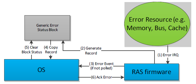
Fig. 18.1 APEI error flow example with external RAS controller
For GHESv2 error sources, the OSPM must acknowledge the consumption of the Error Status Block by writing to the “Read Ack Register” listed in the GHESv2 structure (described in the following table). For platforms that describe multiple Generic Hardware Error Sources, the platform must provide a unique memory region for the Error Status Block of each error source.
Name |
Byte Length |
Byte Offset |
Description |
|---|---|---|---|
Type |
2 |
0 |
10 - Generic Hardware Error Source (version 2) structure |
Equivalent fields in Table 18.10 |
62 |
2 |
Same format as fields in Table 18.10, starting from Source Id and ending in Error Status Block Length (inclusive). |
Read Ack Register |
12 |
64 |
Generic Address Structure as defined in Table 18.10. This field specifies the location of the Read Ack Register used to notify the RAS controller that OSPM has processed the Error Status Block. The OSPM writes the bit(s) specified in Read Ack Write, while preserving the bit(s) specified in Read Ack Preserve. |
Read Ack Preserve |
8 |
76 |
Contains a mask of bits to preserve when writing the Read Ack register. |
Read Ack Write |
8 |
84 |
Contains a mask of bits to set when writing the Read Ack register. |
These are the steps the OS must take once detecting an error from a particular GHESv2 error source:
OSPM detects error (via interrupt/exception or polling the block status)
OSPM copies the error status block
OSPM clears the block status field of the error status block
OSPM acknowledges the error via Read Ack register. For example:
OSPM reads the Read Ack register –> X
OSPM writes –> (( X & ReadAckPreserve) | ReadAckWrite)
18.3.2.9. Hardware Error Notification
This table describes the notification mechanism associated with a hardware error source.
Field |
Byte Length |
Byte Offset |
Description |
|---|---|---|---|
Type |
1 |
0 |
Identifies the notification type:
0 - Polled
1 - External Interrupt
2 - Local Interrupt
3 - SCI
4 - NMI
5 - CMCI
6 - MCE
7 - GPIO-Signal
8 - ARMv8 SEA
9 - ARMv8 SEI
10 - External Interrupt - GSIV
11 - Software Delegated Exception - See Links to ACPI-Related Documents (http://uefi.org/acpi) under the heading, “SDEI Specification.”
All other values are reserved
|
Length |
1 |
1 |
Total length of the structure in bytes. |
Configuration Write Enable |
2 |
2 |
This field indicates whether configuration parameters may be modified by OSPM. If the bit for the associated parameter is set, the parameter is writeable by OSPM:
Bit [0]: Type
Bit [1]: Poll Interval
Bit [2]: Switch To Polling Threshold Value
Bit [3]: Switch To Polling Threshold Window
Bit [4]: Error Threshold Value
Bit [5]: Error Threshold Window All other bits are reserved.
|
Poll Interval |
4 |
4 |
Indicates the poll interval in milliseconds OSPM should use to periodically check the error source for the presence of an error condition. |
Vector |
4 |
8 |
Interrupt vector. For type 10 “External Interrupt - GSIV”, this field specifies the GSIV triggered by the error source. |
Switch To Polling Threshold Value |
4 |
12 |
The number of error interrupts that must occur within Switch To Polling Threshold Interval before OSPM switches the error source to polled mode. |
Switch To Polling Threshold Window |
4 |
16 |
Indicates the time interval in milliseconds that Switch To Polling Threshold Value interrupts must occur within before OSPM switches the error source to polled mode. |
Error Threshold Value |
4 |
20 |
Indicates the number of error events that must occur within Error Threshold Interval before OSPM processes the event as an error condition. |
Error Threshold Window |
4 |
24 |
Indicates the time interval in milliseconds that Error Threshold Value errors must occur within before OSPM processes the event as an error condition. |
18.3.2.10. IA-32 Architecture Deferred Machine Check
Processors implementing the IA-32 Instruction Set Architecture may report Deferred errors to OSPM. These errors indicate that data has been corrupted but not consumed. The information in this table allows platform firmware to communicate key parameters of the deferred processor error reporting mechanism to OSPM, including whether Deferred Machine Check (DMC) processing should be enabled.
Only one entry of this type is permitted in the HEST. OSPM applies the information specified in this entry to all processors.
Field |
Byte Length |
Byte Offset |
Description |
|---|---|---|---|
Type |
2 |
0 |
11 - IA-32 Architecture Deferred Machine Check Structure. |
Source Id |
2 |
2 |
This value serves to uniquely identify this error source against other error sources reported by the platform. |
Reserved |
2 |
4 |
Reserved. |
Flags |
1 |
6 |
Bit [0] - FIRMWARE_FIRST: If set, this bit indicates to the OSPM that system firmware will handle errors from this source first.
Bit [2] - GHES_ASSIST: If set, this bit indicates that although OSPM is responsible for directly handling the error (as expected when FIRMWARE_FIRST is not set), system firmware may report additional information in the context of the error reported by hardware. The additional information is reported in a Generic Hardware Error Source structure with a matching Related Source ID. See Section 18.7, GHES_ASSIST Error Reporting. NOTE: If FIRMWARE_FIRST is set, this bit is reserved.
All other bits must be set to zero.
|
Enabled |
1 |
7 |
If the field value is 1, indicates this error source is to be enabled.
If the field value is 0, indicates that the error source is not to be enabled.
If FIRMWARE_FIRST is set in the flags field, the Enabled field is ignored by OSPM.
|
Number of Records To Pre-allocate |
4 |
8 |
Indicates the number of error records to pre-allocate for this error source. Must be >= 1. |
Max Sections Per Record |
4 |
12 |
Indicates the maximum number of error sections included in an error record created as a result of an error reported by this error source. Must be >= 1. |
Notification Structure |
28 |
16 |
Hardware Error Notification Structure, as defined in Table 18.14. |
Number Of Hardware Banks |
1 |
44 |
Indicates the number of hardware error reporting banks. |
Reserved |
3 |
45 |
Reserved. |
Machine Check Bank Structure[n] |
48 |
A list of Machine Check Bank structures defined in IA-32 Architecture Machine Check Bank Structure. |